MAX189ACWE(2012) View Datasheet(PDF) - Maxim Integrated
Part Name
Description
Manufacturer
MAX189ACWE Datasheet PDF : 18 Pages
| |||
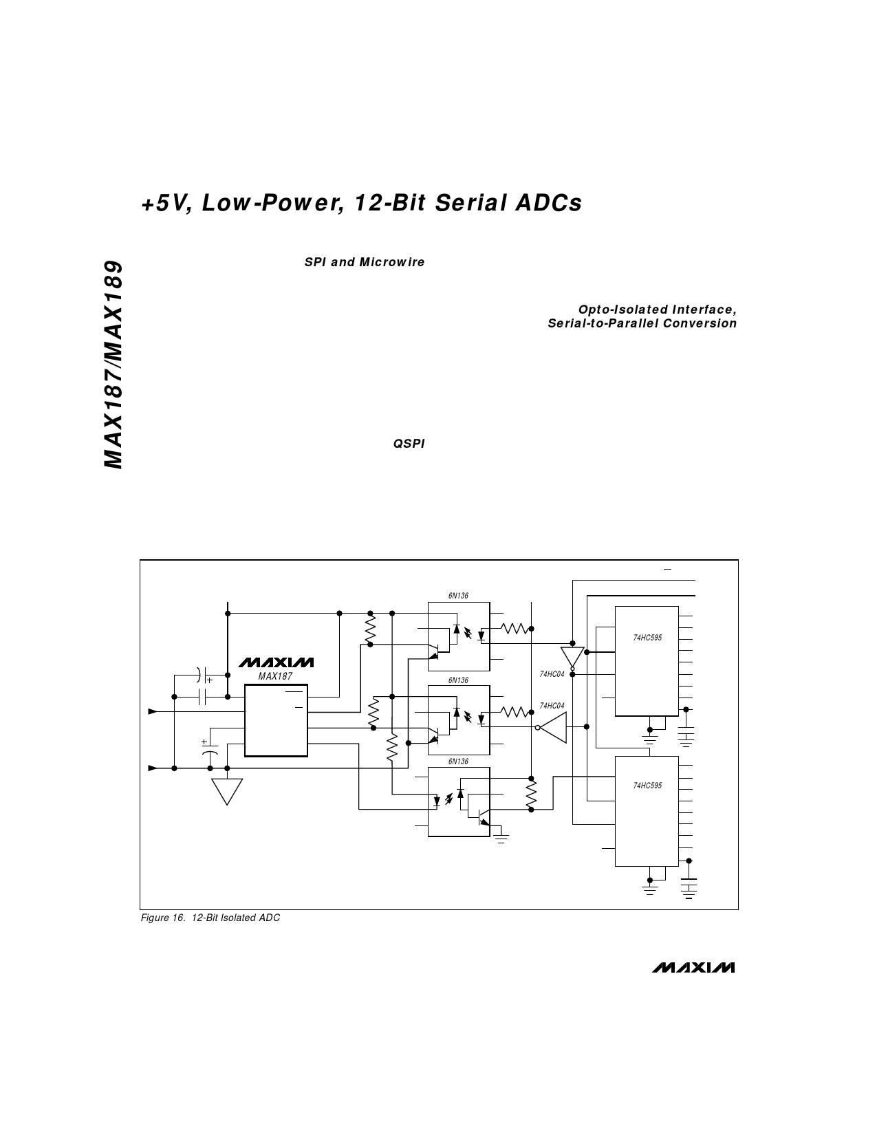
MAX187/ MAX189
+5V, Low-Power, 12-Bit Serial ADCs
Layout, Grounding, Bypassing
For best performance, use printed circuit boards. Wire-
wrap boards are not recommended. Board layout should
ensure that digital and analog signal lines are separated
from each other. Do not run analog and digital (especially
clock) lines parallel to one another, or digital lines under-
neath the ADC package.
Figure 17 shows the recommended system ground con-
nections. A single-point analog ground (“star” ground
point) should be established at GND, separate from the
logic ground. All other analog grounds should be con-
nected to this ground. The 16-pin versions also have a
dedicated DGND pin available. Connect DGND to this
star ground point for further noise reduction. No other
digital system ground should be connected to this single-
point analog ground. The ground return to the power
supply for this ground should be low impedance and as
short as possible for noise-free operation.
High-frequency noise in the VDD power supply may
affect the ADC’s high-speed comparator. Bypass this
supply to the single-point analog ground with 0.01FF
and 4.7FF bypass capacitors. Minimize capacitor lead
lengths for best supply-noise rejection. If the +5V power
supply is very noisy, a 10I resistor can be connected
as a lowpass filter to attenuate supply noise (Figure 17).
SUPPLIES
+5V
GND
R* = 10I
4.7µF
0.01µF
VDD
AGND
MAX187
MAX189
*OPTIONAL
DGND
+5V DGND
DIGITAL
CIRCUITRY
Figure 17. Power-Supply Grounding Condition
Maxim Integrated
16
Share Link: 