LT1220CH View Datasheet(PDF) - Linear Technology
Part Name
Description
Manufacturer
LT1220CH Datasheet PDF : 12 Pages
| |||
LT1220
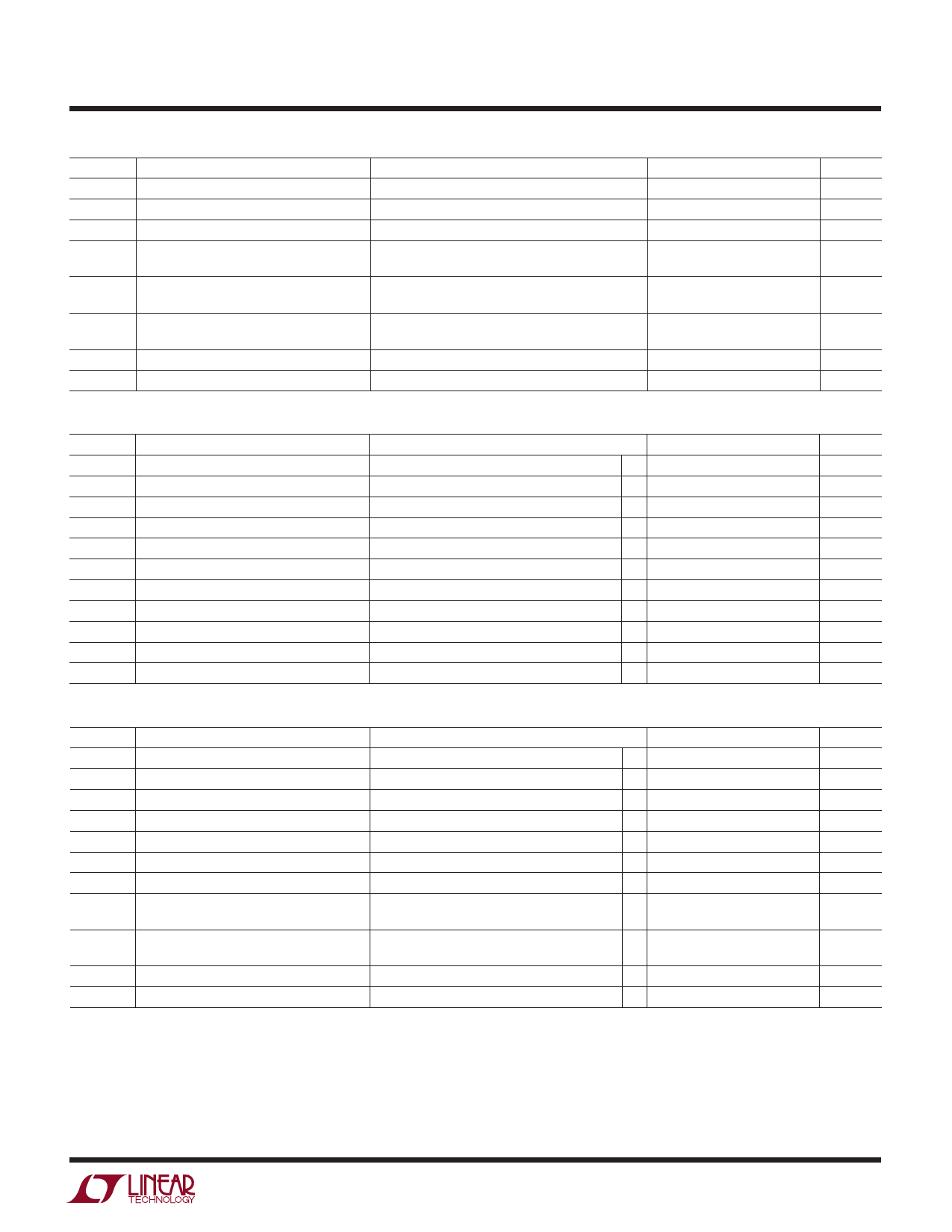
ELECTRICAL CHARACTERISTICS VS = ┬▒15V, TA = 25┬░C, VCM = 0V, unless otherwise specified.
SYMBOL PARAMETER
CONDITIONS
MIN TYP MAX
UNITS
tr, tf
Rise Time, Fall Time
Overshoot
Propagation Delay
ts
Settling Time
AV = 1, 10% to 90%, 0.1V
AV = 1, 0.1V
AV = 1, 50% VIN to 50% VOUT, 0.1V
10V Step, 0.1%
10V Step, 0.01%
2.5
ns
5
%
4.9
ns
75
ns
95
ns
Differential Gain
f = 3.58MHz, RL = 150Ōä” (Note 7)
f = 3.58MHz, RL = 1k (Note 7)
0.10
%
0.02
%
Differential Phase
f = 3.58MHz, RL = 150Ōä” (Note 7)
f = 3.58MHz, RL = 1k (Note 7)
0.20
DEG
0.03
DEG
RO
Output Resistance
AV = 1, f = 1MHz
1
Ōä”
IS
Supply Current
8
10.5
mA
The q denotes the specifications which apply over the temperature range 0┬░C Ōēż TA Ōēż 70┬░C, otherwise specifications are at TA = 25┬░C.
VS = ┬▒15V, VCM = 0V, unless otherwise specified.
SYMBOL PARAMETER
CONDITIONS
MIN TYP MAX
UNITS
VOS
IOS
IB
CMRR
PSRR
AVOL
VOUT
IOUT
SR
IS
Input Offset Voltage
Input VOS Drift
Input Offset Current
Input Bias Current
Common Mode Rejection Ratio
Power Supply Rejection Ratio
Large-Signal Voltage Gain
Output Swing
Output Current
Slew Rate
Supply Current
(Note 4)
VCM = ┬▒12V
VS = ┬▒5V to ┬▒15V
VOUT = ┬▒10V, RL = 500Ōä”
RL = 500Ōä”
VOUT = ┬▒12V
(Note 5)
q
0.5
3.5
q
20
q
100
400
q
100
400
q 92
114
q 86
94
q 20
50
q 12
13
q 24
26
q 180
250
q
8
11
mV
┬ĄV/┬░C
nA
nA
dB
dB
V/mV
┬▒V
mA
V/┬Ąs
mA
The q denotes the specifications which apply over the temperature range ŌĆō 55┬░C Ōēż TA Ōēż 125┬░C, otherwise specifications are at
TA = 25┬░C. VS = ┬▒15V, VCM = 0V, unless otherwise specified.
SYMBOL PARAMETER
CONDITIONS
MIN TYP MAX
UNITS
VOS
IOS
IB
CMRR
PSRR
AVOL
VOUT
IOUT
SR
IS
Input Offset Voltage
Input VOS Drift
Input Offset Current
Input Bias Current
Common Mode Rejection Ratio
Power Supply Rejection Ratio
Large-Signal Voltage Gain
Output Swing
Output Current
Slew Rate
Supply Current
(Note 4)
VCM = ┬▒12V
VS = ┬▒5V to ┬▒15V
VOUT = ┬▒10V, RL = 500Ōä”
RL = 500Ōä”
RL = 1k
VOUT = ┬▒10V
VOUT = ┬▒12V
(Note 5)
q
q
q
q
q 92
q 82
q
5
q 10
q 12
q 20
q 12
q 130
q
0.5
4
20
100
800
100 1000
114
94
50
13
13
26
13
250
8
11
mV
┬ĄV/┬░C
nA
nA
dB
dB
V/mV
┬▒V
┬▒V
mA
mA
V/┬Ąs
mA
Note 1: Absolute Maximum Ratings are those values beyond which the life
of a device may be impaired.
Note 2: A heat sink may be required when the output is shorted indefinitely.
Note 3: Commercial parts are designed to operate over ŌĆō 40┬░C to 85┬░C, but
are not tested nor guaranteed beyond 0┬░C to 70┬░C. Industrial grade parts
specified and tested over ŌĆō40┬░C to 85┬░C are available on special request.
Consult factory.
Note 4: Input offset voltage is pulse tested and is exclusive of warm-up drift.
Note 5: Slew rate is measured between ┬▒10V on an output swing of ┬▒12V.
Note 6: FPBW = SR/2ŽĆVP.
Note 7: Differential Gain and Phase are tested in AV = 2 with five amps in
series. Attenuators of 1/2 are used as loads (75Ōä”, 75Ōä” and 499Ōä”, 499Ōä”).
3
Share Link: 