LTC1273ACS View Datasheet(PDF) - Linear Technology
Part Name
Description
Manufacturer
LTC1273ACS Datasheet PDF : 24 Pages
| |||
LTC1273
LTC1275/LTC1276
APPLICATI S I FOR ATIO
R1
ANALOG 10k
INPUT
+
0V TO 5V
R2
10k 10k
5V
–
R9
20Ω
AIN
R4
100k
R5
4.3k
FULL SCALE
ADJUST
5V
LTC1273
R3
100k
R7
100k
R6
400Ω
R8
10k LTC1273/75/76 • F10b
OFFSET
ADJUST
R1
ANALOG 10k
INPUT
±2.5V (LTC1275)
±5V (LTC1276)
+
R2
10k
–
AIN
R4
100k
R5
4.3k
FULL SCALE
ADJUST 5V
LTC1275
LTC1276
R3
100k
R7
100k
R6
200Ω
R8
20k LTC1273/75/76 • F10c
OFFSET
ADJUST
– 5V
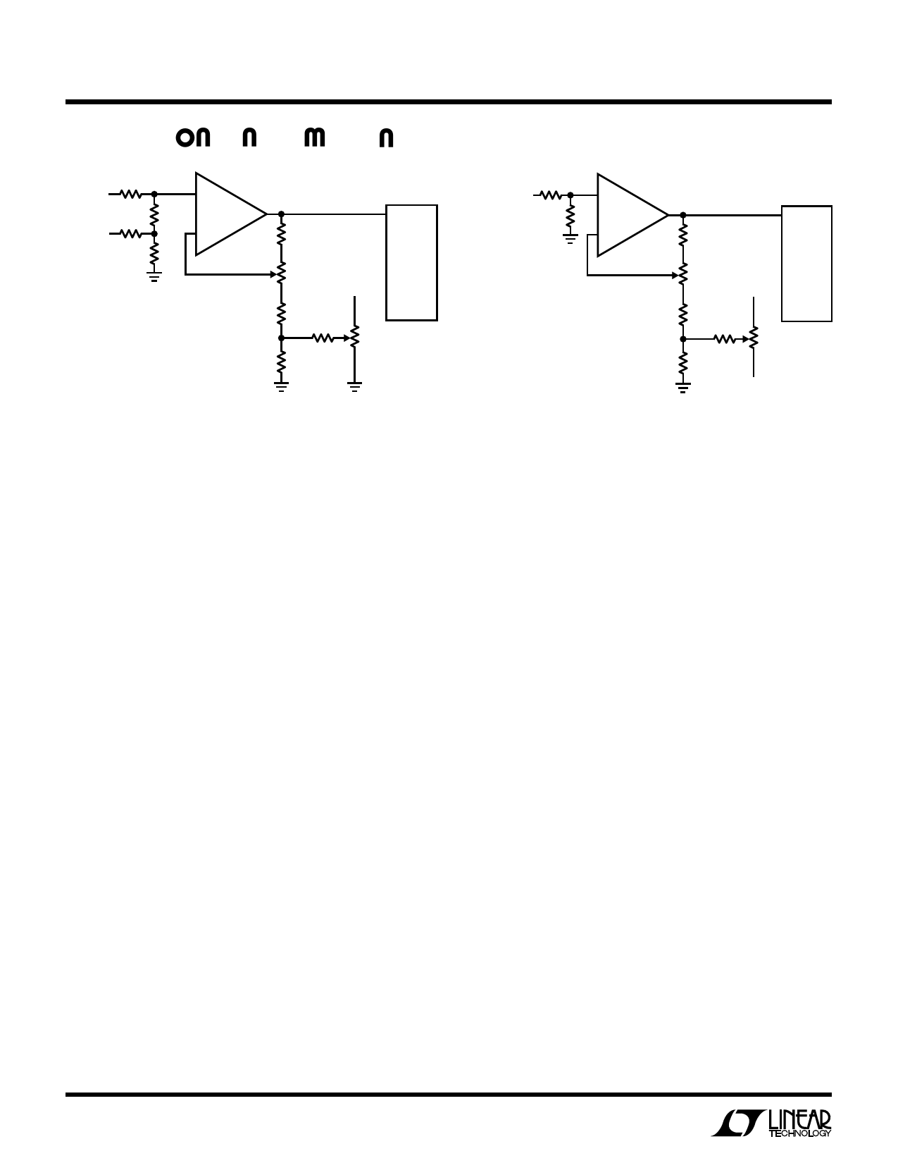
Figure 10b. LTC1273 Offset and Full Scale Adjust Circuit
should be adjusted before full scale. To adjust offset, apply
0.61mV (i.e., 1/2LSB) at the input and adjust the offset trim
until the LTC1273 output code flickers between 0000 0000
0000 and 0000 0000 0001. To adjust full scale, apply an
analog input of 4.99817V (i.e., FS – 1 1/2LSBs or last code
transition) at the input and adjust the full scale trim until
the LTC1273 output code flickers between 1111 1111
1110 and 1111 1111 1111. It should be noted that if
negative ADC offsets need to be adjusted or if an output
swing to ground is required, the op amp in Figure 10b
requires a negative power supply.
Bipolar Offset and Full Scale Adjustment
(LTC1275/LTC1276)
Bipolar offset and full scale errors are adjusted in a similar
fashion to the unipolar case. Figure 10a shows the extra
components required for full scale error adjustment. If both
offset and full scale adjustments are needed, the circuit in
Figure 10c can be used. Again, bipolar offset must be
adjusted before full scale error. Bipolar offset adjustment is
achieved by trimming the offset adjustment of Figure 10c
while the input voltage is 1/2LSB below ground. This is done
by applying an input voltage of – 0.61mV or – 1.22mV
(– 0.5LSB for LTC1275 or LTC1276) to the input in Figure
10c and adjusting R8 until the ADC output code flickers
between 0000 0000 0000 and 1111 1111 1111. For full
scale adjustment, an input voltage of 2.49817V or 4.99636V
(FS – 1 1/2LSBs for LTC1275 or LTC1276) is applied to the
Figure 10c. LTC1275/LTC1276 Offset and
Full Scale Adjust Circuit
input and R5 is adjusted until the output code flickers
between 0111 1111 1110 and 0111 1111 1111.
BOARD LAYOUT AND BYPASSING
The LTC1273/LTC1275/LTC1276 are easy to use. To ob-
tain the best performance from the devices a printed
circuit board is required. Layout for the printed circuit
board should ensure that digital and analog signal lines are
separated as much as possible. In particular, care should
be taken not to run any digital track alongside an analog
signal track. The analog input should be screened by
AGND.
High quality tantalum and ceramic bypass capacitors
should be used at the VDD and VREF pins as shown in Figure
11. For the LTC1275/LTC1276 a 0.1µF ceramic provides
adequate bypassing for the VSS pin. The capacitors must
be located as close to the pins as possible. The traces
connecting the pins and the bypass capacitors must be
kept short and should be made as wide as possible.
Noise: Input signal leads to AIN and signal return leads
from AGND (Pin 3) should be kept as short as possible to
minimize input noise coupling. In applications where this
is not possible, a shielded cable between source and ADC
is recommended. Also, since any potential difference in
grounds between the signal source and ADC appears as an
14
Share Link: 