MAQ5282YMME View Datasheet(PDF) - Micrel
Part Name
Description
Manufacturer
MAQ5282YMME Datasheet PDF : 16 Pages
| |||
Micrel, Inc.
MAQ5282
Absolute Maximum Ratings(1)
VIN to GND................................................... –0.3V to +125V
VCPSRR to GND..................................................–0.3 to +14V
VFB, VSNS, VOUT to GND ................................... –0.3V to +6V
Power Dissipation (PD) ........................... Internally Limited(3)
Lead Temperature (soldering, 10s).......................... +260°C
Junction Temperature ......................... –40°C ≤ TJ ≤ +125°C
Storage Temperature .........................–65°C ≤ TA ≤ +150°C
ESD Ratings(4)
HBM ......................................................................... 2kV
MM ......................................................................... 200V
Operating Ratings(2)
VIN ................................................................. +6V to +120V
VOUT Adjust Range ..................................... +1.27V to +5.5V
Junction Temperature ......................... –40°C ≤ TJ ≤ +125°C
Junction Thermal Resistance (θJA)
8-pin ePad MSOP..............................................64°C/W
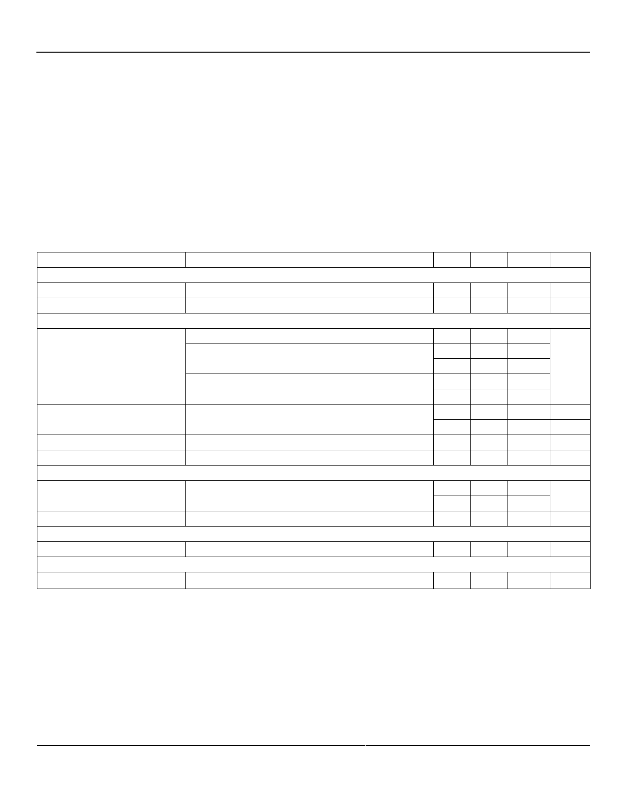
Electrical Characteristics(5)
VIN = 12V, CIN = 1.0µF, CPSRR = 0.1µF, COUT = 10µF, IOUT = 100µA, TA = 25°C, bold values indicate –40°C ≤ TJ ≤ +125°C, unless noted.
Parameter
Condition
Min. Typ. Max. Units
Power Supply Input
Input Voltage Range(6)
Quiescent Supply Current(7)
IOUT = 0
6
120
V
6
11
µA
Output Voltage
Adjustable
1.27
5.5
Output Voltage
Fixed 3.3V
3.2
3.3
3.4
3.13 3.3
3.47
V
Fixed 5.0V
4.85 5.0
5.15
4.75 5.0
5.25
Output Voltage Accuracy
Variation from nominal VOUT
-3
+3
%
-5
+5
%
Load Regulation
Line Regulation(8)
IOUT = 100µA to 50mA
VIN = 10V to 120V
-1.0 0.5
+1.0
%
-0.5 0.04 +0.5
%/V
Feedback Input (Adjustable)
FB Voltage
1.232 1.270 1.308
V
1.206 1.270 1.333
FB Current
VFB = 1.27V
3.2
nA
Current Limit
Current Limit
VOUT = 0V
60
125
260
mA
Ripple Rejection
Power Supply Rejection Ratio
f = 20kHz to 1MHz
80
dB
Notes:
1. Exceeding the absolute maximum rating may damage the device.
2. The device is not guaranteed to function outside its operating rating.
3. The maximum allowable power dissipation at any TA (ambient temperature) is PD(max) = (TJ(max) – TA) / θJA. Exceeding the maximum allowable power
dissipation results in excessive die temperature, and causes the regulator to enter thermal shutdown.
4. Devices are ESD sensitive; use proper handling precautions. Human body model, 1.5kΩ in series with 100pF.
5. Specifications are for packaged products only.
6. Assure that VIN ≥ (VOUT + 3V) and VIN ≥ 6V.
7. Quiescent current is specified for the adjustable option. The fixed options will add approximately 1µA due to the internal feedback resistors.
8. Line regulation is a percentage of VOUT.
October 2, 2014
3
Revision 2.0
Share Link: 