MAX4172EUA(2012) View Datasheet(PDF) - Maxim Integrated
Part Name
Description
Manufacturer
MAX4172EUA Datasheet PDF : 9 Pages
| |||
MAX4172
Low-Cost, Precision, High-Side
Current-Sense Amplifier
flows through RG1, IRG1 x RG1 = ILOAD x RSENSE. The
internal current mirror multiplies IRG1 by a factor of 50
to give IOUT = 50 x IRG1. Substituting IOUT/50 for IRG1,
(IOUT/50) x RG1 = ILOAD x RSENSE, or:
IOUT = 50 x ILOAD x (RSENSE/RG1)
The internal current gain of 50 and the factory-trimmed
resistor RG1 combine to result in the MAX4172
transconductance (Gm) of 10mA/V. Gm is de-
fined as being equal to IOUT/(VRS+ - VRS-). Since (VRS+
- VRS-) = ILOAD x RSENSE, the output current (IOUT) can
be calculated with the following formula:
IOUT = Gm x (VRS+ - VRS-) =
(10mA/V) x (ILOAD x RSENSE)
Current Output
The output voltage equation for the MAX4172 is given
below:
VOUT = (Gm) x (RSENSE x ROUT x ILOAD)
where VOUT = the desired full-scale output voltage,
ILOAD = the full-scale current being sensed, RSENSE =
the current-sense resistor, ROUT = the voltage-setting
resistor, and Gm = MAX4172 transconductance
(10mA/V).
The full-scale output voltage range can be set by
changing the ROUT resistor value, but the output volt-
age must be no greater than V+ - 1.2V. The above
equation can be modified to determine the ROUT
required for a particular full-scale range:
ROUT = (VOUT)/(ILOAD x RSENSE x Gm)
OUT is a high-impedance current source that can be
integrated by connecting it to a capacitive load.
PG Output
The PG output is an open-collector logic output that
indicates the status of the MAX4172’s V+ power sup-
ply. A logic low on the PG output indicates that V+ is
sufficient to power the MAX4172. This level is tempera-
ture dependent (see Typical Operating Characteristics
graphs), and is typically 2.7V at room temperature. The
internal PG comparator has a 100mV (typical) hystere-
sis to prevent possible oscillations caused by repeated
toggling of the PG output, making the device ideal for
power-management systems lacking soft-start capabili-
ty. An internal delay (15µs typical) in the PG compara-
tor allows adequate time for power-on transients to
settle out. The PG status indicator greatly simplifies the
design of closed-loop systems by ensuring that the
components in the control loop have sufficient voltage
to operate correctly.
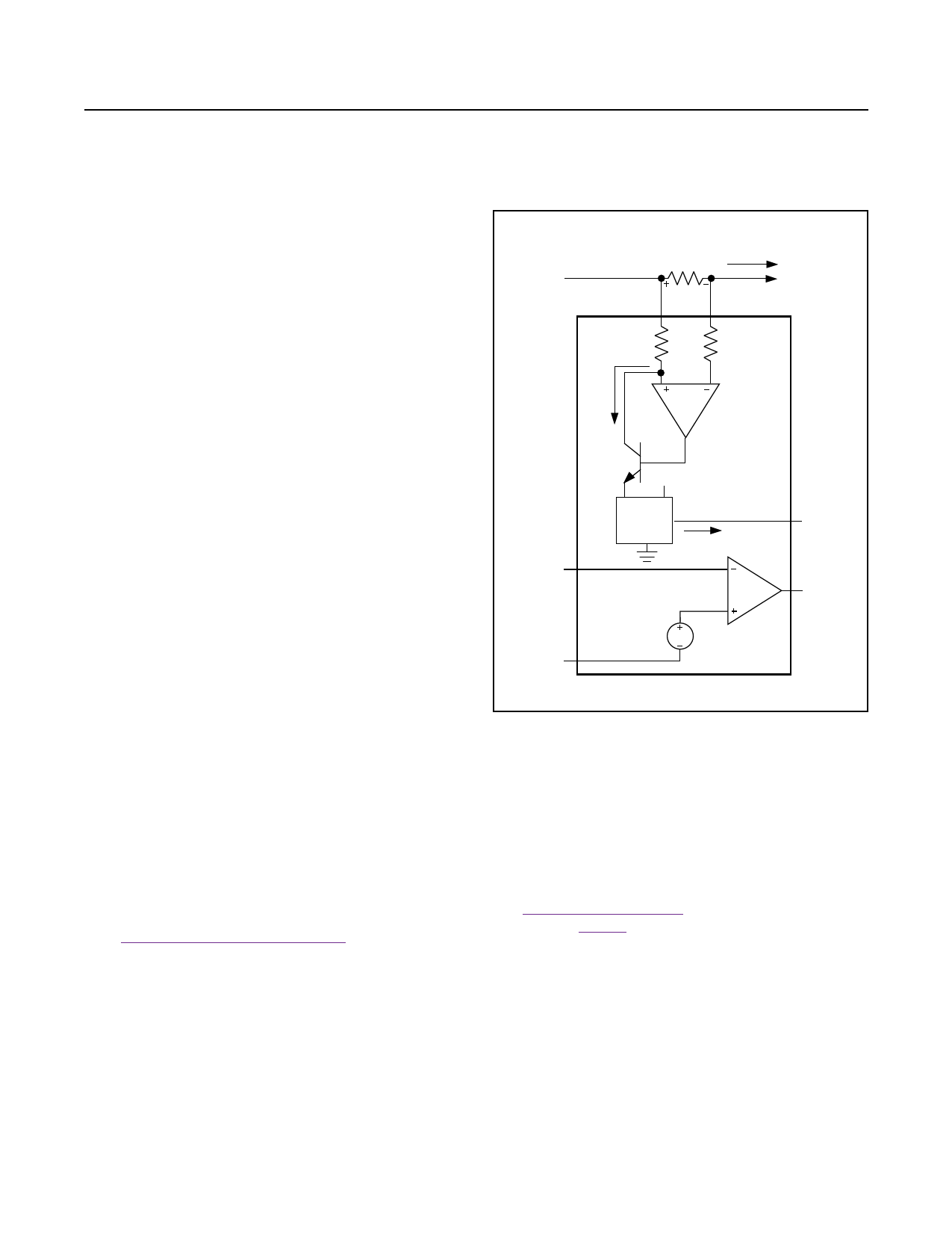
INPUT
RSENSE
ILOAD
RS+ VSENSE RS-
TO LOAD/
BATTERY
RG1
RG2
IRG1
A1
Q1
V+
MAX4172
1:50
CURRENT
IOUT = 50 IRG1
OUT
MIRROR
V+
PG
VTH
GND
Figure 1. Functional Diagram
__________Applications Information
Suggested Component Values
for Various Applications
The Typical Operating Circuit is useful in a wide variety
of applications. Table 1 shows suggested component
values and indicates the resulting scale factors for vari-
ous applications required to sense currents from
100mA to 10A.
Adjust the RSENSE value to monitor higher or lower cur-
rent levels. Select RSENSE using the guidelines and for-
mulas in the following section.
Sense Resistor, RSENSE
Choose RSENSE based on the following criteria:
• Voltage Loss: A high RSENSE value causes the
power-source voltage to degrade through IR loss.
For minimal voltage loss, use the lowest RSENSE
value.
6
Maxim Integrated
Share Link: 