MB88346BPF View Datasheet(PDF) - Fujitsu
Part Name
Description
Manufacturer
MB88346BPF Datasheet PDF : 18 Pages
| |||
MB88346B
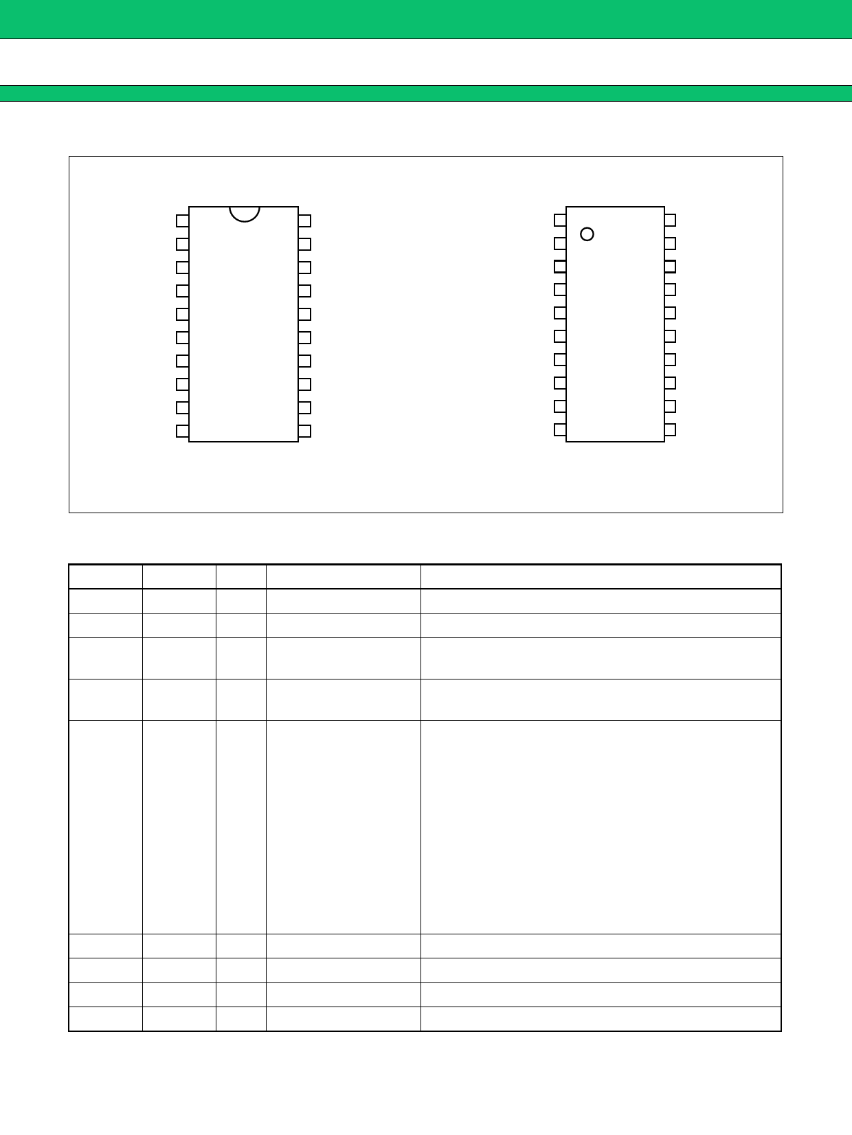
■ PIN ASSIGNMENTS
(TOP VIEW)
VSS
AO3
AO4
AO5
AO6
AO7
AO8
AO9
AO10
VDD
1
20
2
19
3
18
4
17
5
16
6
15
7
14
8
13
9
12
10
11
(DIP-20P-M02)
GND
AO2
AO1
DI
CLK
LD
DO
AO12
AO11
VCC
(TOP VIEW)
VSS 1
AO3 2
AO4 3
AO5 4
AO6 5
AO7 6
AO8 7
AO9 8
AO10 9
VDD 10
20 GND
19 AO2
18 AO1
17 DI
16 CLK
15 LD
14 DO
13 AO12
12 AO11
11 VCC
(FPT-20P-M01)
(FPT-20P-M03)
■ PIN DESCRIPTION
Pin No. Symbol I/O
Pin name
Function
17
DI*
I Data input pin
This pin inputs 12-bit serial data.
14
DO
O Data output pin
This pin outputs MSB bit data of 12-bit shift register.
16
CLK*
I Shift clock input pin
Input signal from DI pin is inputted to 12-bit shift register
at rising of shift clock.
15
LD*
I
Load signal input pin
If input “H” level to LD pin, the data of 12-bit shift register
is loaded to the decoder and the register for D/A output.
18,
AO1,
19,
AO2,
2,
AO3,
3,
AO4,
4,
AO5,
5,
6,
AO6,
AO7,
O D/A output pin
7,
AO8,
8,
AO9,
9,
AO10,
12,
AO11,
13
AO12
These pins output analog data of 8-bit D/A converter with
OP amplifier.
11
VCC
⎯ Power supply pin
Power supply pin of MCU interface and OP amplifier
20
GND
⎯ Ground pin
Ground pin of MCU interface and OP amplifier
10
VDD
⎯ Power supply pin
Power supply pin of D/A converter
1
VSS
⎯ Ground pin
Ground pin of D/A converter
* : When three pins, DI, CLK, and LD pins are connected to 3-V MCU, they are fixed to “L” level at non transfer.
3
Share Link: 