MC74LVX02(2011) View Datasheet(PDF) - ON Semiconductor
Part Name
Description
Manufacturer
MC74LVX02 Datasheet PDF : 7 Pages
| |||
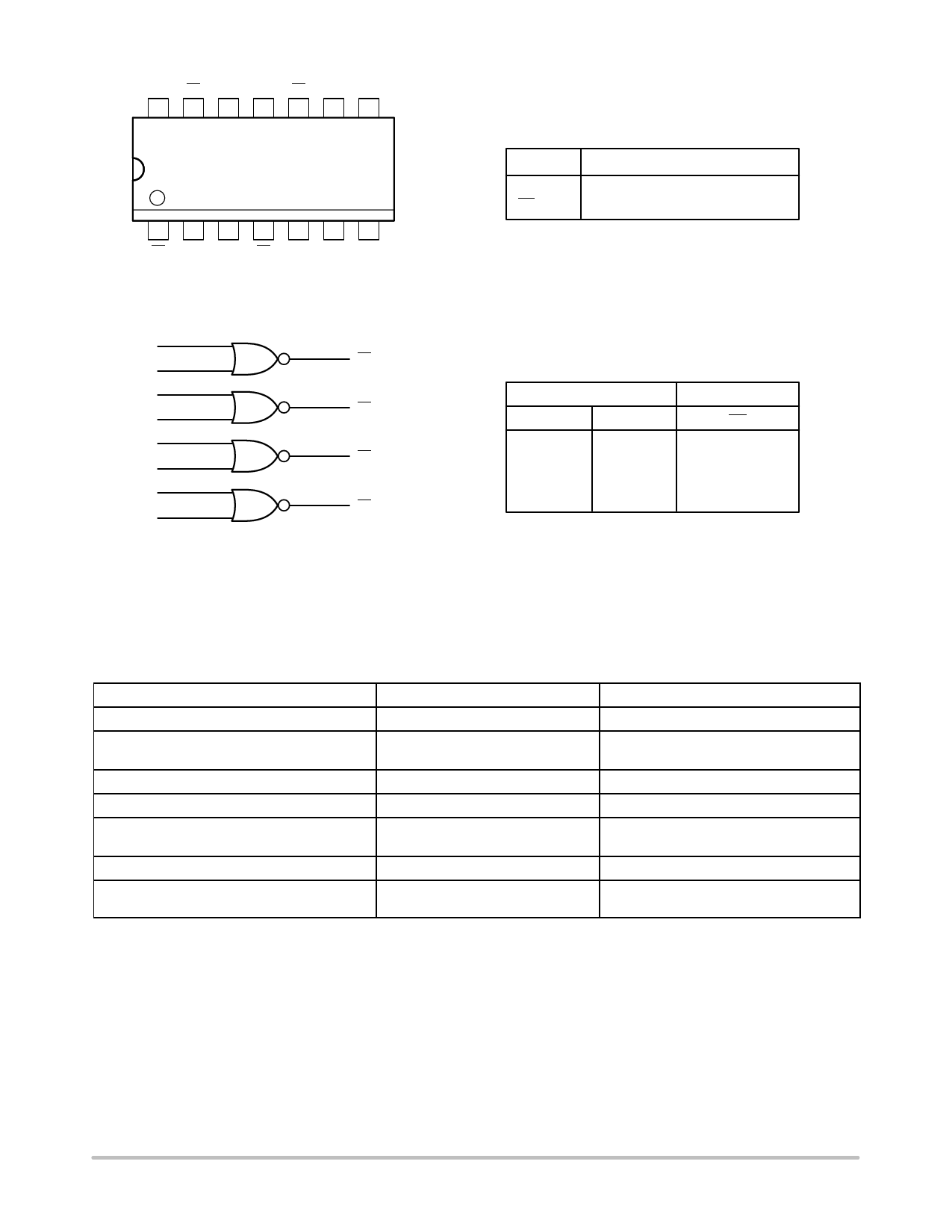
MC74LVX02
VCC O2 B2 A2 O3 B3 A3
14 13 12 11 10 9 8
1234567
O0 A0 B0 O1 A1 B1 GND
Figure 1. Figure 1. 14−Lead Pinout (Top View)
PIN NAMES
Pins
Function
An, Bn
On
Data Inputs
Outputs
2
A0
3
B0
5
A1
6
B1
11
A2
12
B2
8
A3
9
B3
1
O0
4
O1
13
O2
10
O3
Figure 2. Figure 2. Logic Diagram
FUNCTION TABLE
INPUTS
An
Bn
L
L
L
H
H
L
H
H
OUTPUTS
On
H
L
L
L
ORDERING INFORMATION
Device
Package
Shipping†
MC74LVX02DR2G
SOIC−14
(Pb−Free)
2500 Tape & Reel
MC74LVX02DTR2G
TSSOP−14*
2500 Tape & Reel
MC74LVX02MG
SOEIAJ−14
(Pb−Free)
50 Units / Rail
MC74LVX02MELG
SOEIAJ−14
(Pb−Free)
2000 Tape & Reel
†For information on tape and reel specifications, including part orientation and tape sizes, please refer to our Tape and Reel Packaging
Specifications Brochure, BRD8011/D.
*This package is inherently Pb−Free.
http://onsemi.com
2
Share Link: 