MCP1602T-150I/MS View Datasheet(PDF) - Microchip Technology
Part Name
Description
Manufacturer
MCP1602T-150I/MS Datasheet PDF : 26 Pages
| |||
MCP1602
3.0 PIN DESCRIPTIONS
The descriptions of the pins are listed in Table 3-1.
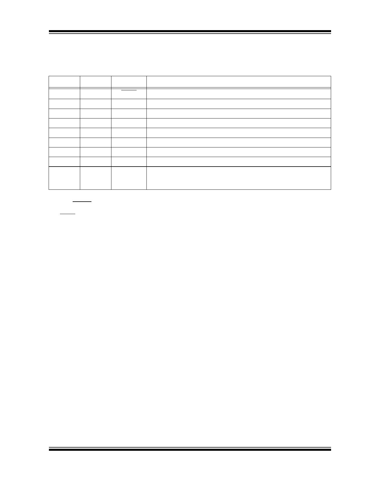
TABLE 3-1: PIN FUNCTION TABLE
MSOP
DFN
Sym
Description
1
1
SHDN Shutdown Input Pin
2
2
VCC
Analog Input Supply Voltage Pin
3
3
PG
Power Good Output Pin
4
4
AGND Analog Ground Pin
5
5
VFB/VOUT Feedback Voltage (Adjustable Version) / Output Voltage (Fixed Version) Pin
6
6
VIN
Input Supply Voltage Pin
7
7
LX
Buck Inductor Output Pin
8
8
PGND Power Ground Pin
—
Exposed
Pad
EP
For the DFN package, the center exposed pad is a thermal path to remove
heat from the device. Electrically this pad is at ground potential and should
be connected to AGND
3.1 Shutdown Control Input Pin
(SHDN)
The SHDN pin is a logic-level input used to enable or
disable the device. A logic high (>45% of VIN) will
enable the regulator output. A logic-low (<15% of VIN)
will ensure that the regulator is disabled.
3.2 Analog Input Supply Voltage Pin
(VCC)
The VCC pin provides bias for internal analog functions.
This voltage is derived by filtering the VIN supply.
3.3 Power-Good Output Pin (PG)
PG is an output level indicating that the output voltage
is within 94% of regulation. The PG output is configured
as an open-drain output.
3.4 Analog Ground Pin (AGND)
AGND is the analog ground connection. Tie AGND to the
analog portion of the ground plane (AGND). See the
physical layout information in the Section 5.8 “PCB
Layout Information” section for ground recommenda-
tions.
3.6 Power Supply Input Voltage Pin
(VIN)
VIN is the buck regulator power input supply pin.
Connect a variable input voltage source to VIN.
3.7 Buck Inductor Output Pin (LX)
Connect LX directly to the buck inductor. This pin
carries large signal-level current; all connections
should be made as short as possible.
3.8 Power Ground Pin (PGND)
Connect all large signal level ground returns to PGND.
These large signal level ground traces should have a
small loop area and length to prevent coupling of
switching noise to sensitive traces.
3.9 Exposed Metal Pad (EP)
For the DFN package, connect the Exposed Pad to
AGND, with vias into the AGND plane. This connection to
the AGND plane will aid in heat removal from the
package.
3.5 Output Voltage Sense Pin (VFB/
VOUT)
For the adjustable output voltage options, connect the
center of the output voltage divider to the VFB pin. For
fixed-output voltage options, connect the output of the
buck regulator to this pin (VOUT).
© 2007 Microchip Technology Inc.
DS22061A-page 11
Share Link: 