NCP1219 View Datasheet(PDF) - ON Semiconductor
Part Name
Description
Manufacturer
NCP1219 Datasheet PDF : 20 Pages
| |||
NCP1219
Vskip/latch
9.5 V (maximum pin voltage)
Controller is latched
Vlatch
Skip threshold clamped to Vskip(MAX)
Vskip(MAX)(maximum skip threshold)
Adjustable Vskip range.
0 V (no skip)
Within the adjustable Vskip range, the skip level changes
according to Equation 10.
Vskip
+
2 V @ (Rlower
(Rlower ø Rskip)
ø Rskip)
) Rupper
(eq. 10)
An internal clamp limits the skip threshold (Vskip(MAX))
to 1.3 V. Increasing the voltage on the Skip/latch pin
beyond the value of the internal clamp will induce no
further change in the skip level. This prevents the act of
disabling the controller in the presence of an external latch
event from causing it to enter skip mode. The relationship
between %ICSSKIP, VSkip/latch, Vskip, and Rskip is
summarized in Table 4.
Figure 39. NCP1219 VSkip/latch Pin Operating
Regions
Table 4. %ICSskip and Skip Threshold Relationship with Rskip
%ICSskip
VSkip/latch
Vskip
Rskip
0%
0V
0V
0W
12%
0.36 V
0.36 V
11.8 kW
25%
0.75 V
0.75 V
52.3 kW
37%
1.10 V
1.10 V
Open
43%
2.00 V
1.30 V
–
43 %
3.00 V
1.30 V
–
Comment
Never skips
–
–
Default Skip Threshold
No further increase in Skip threshold
No further increase in Skip threshold
External Non−Latched Shutdown
Figure 40 summarizes the operating regions of the FB
pin. An external non−latched shutdown can be easily
implemented by simply pulling FB below the skip level.
This is an inherent feature of the standby skip operation,
allowing additional flexibility in the SMPS design.
V FB
Fault operation when staying
in this region longer than 118 ms
3V
PWM operation
V skip
0V
No DRV pulses
Figure 40. NCP1219 Operation Threshold
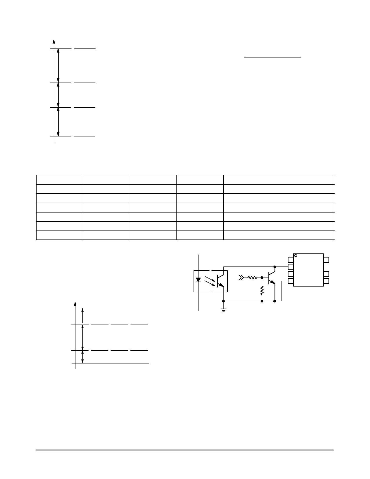
Figure 41 shows an example implementation of a
non−latched shutdown circuit using a bipolar transistor to
pull the FB pin low.
OFF
opto
coupler
Skip/latch HV
FB
CS
VCC
GND DRV
NCP1219
Figure 41. Example Circuit for Non−Latched
Shutdown
Overload Protection
Figure 42 details the timer based fault detection circuitry.
When an overload (or short circuit) event occurs, the output
voltage collapses and the optocoupler does not conduct
current. This opens the FB pin and VFB is internally pulled
higher than 3.0 V. Since VFB/3 is greater than 1 V, the
controller activates an error flag and starts a timer, tOVLD
(118 ms typical). If the output recovers during this time, the
timer is reset and the device continues to operate normally.
http://onsemi.com
18
Share Link: 