NCP1608 View Datasheet(PDF) - ON Semiconductor
Part Name
Description
Manufacturer
NCP1608 Datasheet PDF : 24 Pages
| |||
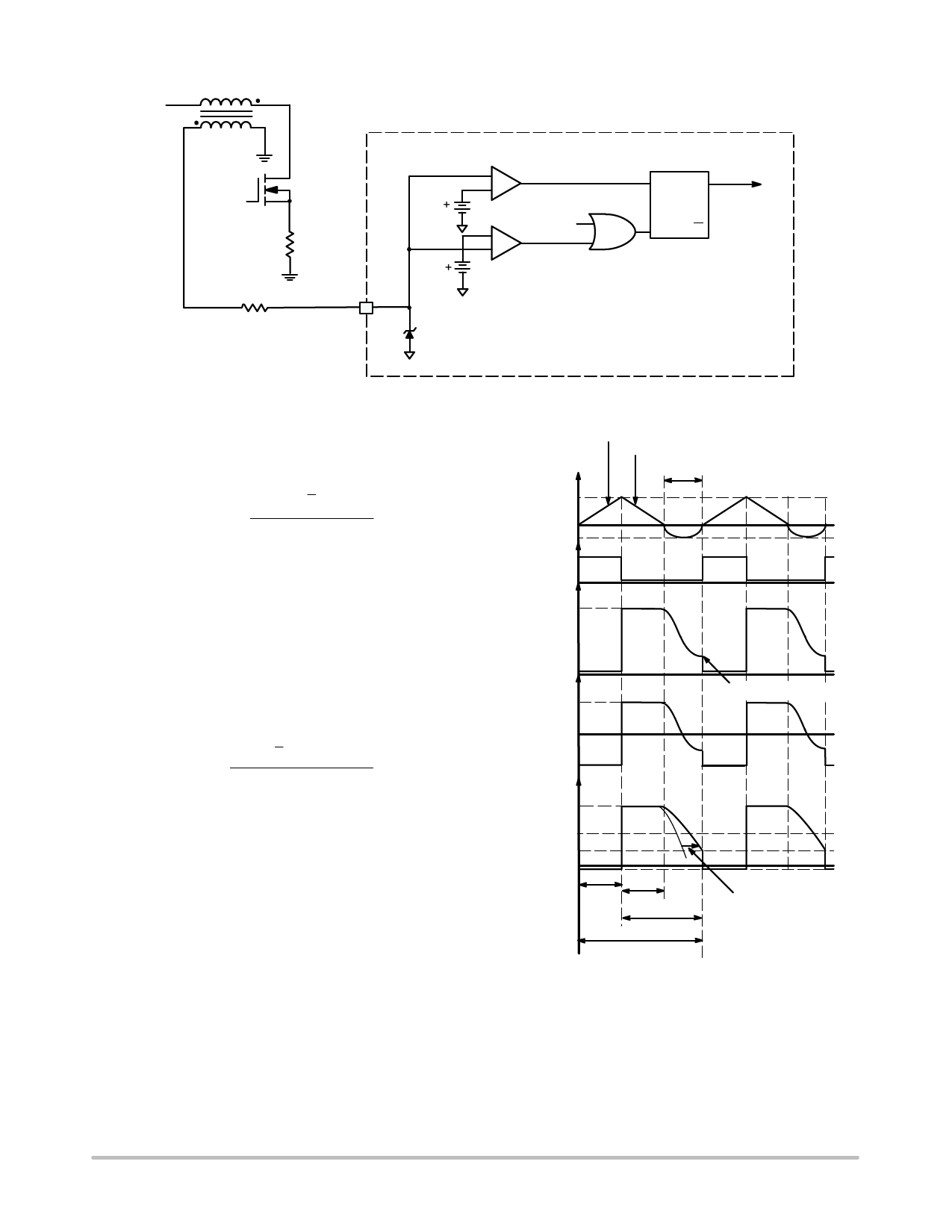
NB
Vin
NZCD
Rsense
RZCD
ZCD
NCP1608
+
−
VZCD(ARM)
DRIVE
+
−
VZCD(TRIG)
ZCD Clamp
SQ
Reset
Dominant
Latch
RQ
Demag
Figure 33. Implementation of the ZCD Block
This sequence achieves CrM operation. The maximum
VZCD(ARM) sets the maximum turns ratio and is calculated
using Equation 11:
ǒ Ǔ NB
:
NZCD
v
Vout
* Ǹ2 @ VacHL
VZCD(ARM)
(eq. 11)
Where VacHL is the maximum rms input voltage and
VZCD(ARM) = 1.55 V (maximum value).
The NCP1608 prevents excessive voltages on the ZCD
pin by clamping VZCD. When the ZCD winding is negative,
the ZCD pin is internally clamped to VCL(NEG). Similarly,
when the ZCD winding is positive, the ZCD pin is
internally clamped to VCL(POS). A resistor (RZCD in
Figure 33) is necessary to limit the current into the ZCD
pin. The maximum ZCD pin current (IZCD(MAX)) is limited
to less than 10 mA. RZCD is calculated using Equation 12:
RZCD
w
Ǹ2 @ VacHL
IZCD(MAX) @ (NB : NZCD)
(eq. 12)
The value of RZCD and the parasitic capacitance of the
ZCD pin determine when the ZCD winding signal is
detected and the drive turn on begins. A large RZCD value
creates a long delay before detecting the ZCD event. In this
case, the controller operates in DCM and the power factor
is reduced. If the RZCD value is too small, the drive turns
on when the drain voltage is high and efficiency is reduced.
A popular strategy for selecting RZCD is to use the RZCD
value that achieves minimum drain voltage turn on. This
value is found experimentally. Figure 34 shows the realistic
waveforms for CrM operation due to RZCD and the ZCD pin
capacitance.
MOSFET Conduction
Diode Conduction
IL
tz
IL(peak)
IL(NEG)
0A
DRV
0V
Vdrain
Vout
VZCD(WIND)
VZCD(WIND),off
VZCD(WIND),on
VZCD
VCL(POS)
VZCD(ARM)
VZCD(TRIG)
VCL(NEG)
ton
tdiode
toff
0V
Minimum Voltage Turn on
0V
0V
RZCD Delay
TSW
Figure 34. Realistic CrM Waveforms Using a ZCD
Winding with RZCD and the ZCD Pin Capacitance
http://onsemi.com
15
Share Link: 