NCV4290 View Datasheet(PDF) - ON Semiconductor
Part Name
Description
Manufacturer
NCV4290 Datasheet PDF : 16 Pages
| |||
NCV4290
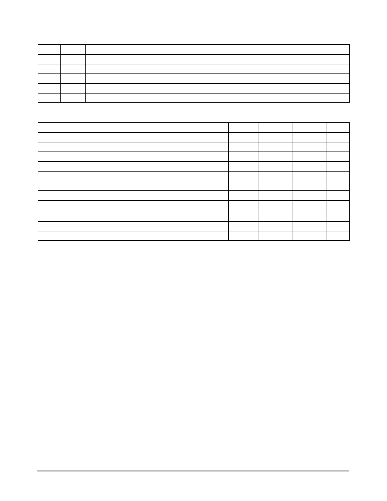
PIN FUNCTION DESCRIPTION
Pin #
ÑÑÑÑÑÑÑÑÑÑÑÑÑÑÑÑÑÑÑÑÑÑÑÑÑÑÑÑÑÑÑÑÑ 1
ÑÑÑÑÑÑÑÑÑÑÑÑÑÑÑÑÑÑÑÑÑÑÑÑÑÑÑÑÑÑÑÑÑ 2
ÑÑÑÑÑÑÑÑÑÑÑÑÑÑÑÑÑÑÑÑÑÑÑÑÑÑÑÑÑÑÑÑÑ 3, Tab
ÑÑÑÑÑÑÑÑÑÑÑÑÑÑÑÑÑÑÑÑÑÑÑÑÑÑÑÑÑÑÑÑÑ 4
ÑÑÑÑÑÑÑÑÑÑÑÑÑÑÑÑÑÑÑÑÑÑÑÑÑÑÑÑÑÑÑÑÑÑÑÑÑÑÑÑÑÑÑÑÑÑÑÑÑÑÑÑÑÑÑÑÑÑÑÑÑÑÑÑÑÑ 5
Symbol
Description
I
Input; Battery Supply Input Voltage. Bypass to ground with a ceramic capacitor.
PG
GND
Power Good Output; Open Collector Active Power Good (accurate when VQ > 1.0 V).
Ground; Pin 3 internally connected to tab.
D
Power Good Delay; timing capacitor to GND for Power Good Delay function.
Q
Output; ±2.0%, 450 mA output. Bypass with 22 mF capacitor, ESR < 4.0 W.
MAXIMUM RATINGS
Rating
Symbol
Min
Max
Unit
Input Voltage
VI
−42
45
V
Input Peak Transient Voltage
VI
−
45
V
Output Voltage
VQ
−1.0
16
V
Power Good Output Voltage
VPG
−0.3
25
V
Power Good Output Current
IPG
−5.0
5.0
mA
Power Good Delay Voltage
VD
−0.3
7.0
V
Power Good Delay Current
ID
−2.0
2.0
mA
ESD Susceptibility (Note 1) − Human Body Model
− Machine Model
− Charge Device Model
ESDHBM
ESDMM
ESDCDM
4.0
200
1000
−
kV
−
V
−
V
Junction Temperature
TJ
−40
150
°C
Storage Temperature
Tstg
−55
150
°C
Stresses exceeding Maximum Ratings may damage the device. Maximum Ratings are stress ratings only. Functional operation above the
Recommended Operating Conditions is not implied. Extended exposure to stresses above the Recommended Operating Conditions may affect
device reliability.
1. This device incorporates ESD protection and is tested by the following methods: ESD Human Body Model tested per AEC−Q100−002, ESD
Machine Model tested per AEC−Q100−003, ESD Charged Device Model tested per AEC−Q100−011, Latch−up tested per AEC−Q100−004.
http://onsemi.com
2
Share Link: 