NCV8450(2010) View Datasheet(PDF) - ON Semiconductor
Part Name
Description
Manufacturer
NCV8450
(Rev.:2010)
(Rev.:2010)
ON Semiconductor
NCV8450 Datasheet PDF : 9 Pages
| |||
NCV8450
MAXIMUM RATINGS
Value
Rating
Symbol
Min
Max
Unit
DC Supply Voltage (Note 1)
Load Dump Protection
(RI = 2 W, td = 400 ms, VIN = 0, 10 V, IL = 150 mA, Vbb = 13.5 V)
Input Current
Output Current (Note 1)
Total Power Dissipation
@ TA = 25°C (Note 2)
@ TA = 25°C (Note 3)
Electrostatic Discharge (Note 4)
(Human Body Model (HBM) 100 pF/1500 W)
Input
All other
VD
VLoaddump
Iin
Iout
PD
−16
45
V
100
V
−15
15
mA
Internally Limited
A
W
1.13
1.60
kV
1
5
Single Pulse Inductive Load Switching Energy (Note 4)
EAS
(VDD = 13.5 V, I = 465 mApk, L = 200 mH, TJStart = 150°C)
29
mJ
Operating Junction Temperature
TJ
−40
+150
°C
Storage Temperature
Tstorage
−55
+150
°C
Stresses exceeding Maximum Ratings may damage the device. Maximum Ratings are stress ratings only. Functional operation above the
Recommended Operating Conditions is not implied. Extended exposure to stresses above the Recommended Operating Conditions may affect
device reliability.
1. Reverse Output current has to be limited by the load to stay within absolute maximum ratings and thermal performance.
2. Minimum Pad.
3. 1 in square pad size, FR−4, 1 oz Cu.
4. Not subjected to production testing.
THERMAL RESISTANCE RATINGS
Parameter
Thermal Resistance (Note 5)
Junction−to−Ambient (Note 2)
Junction−to−Ambient (Note 3)
5. Not subjected to production testing.
Symbol
RqJA
RqJA
Max Value
110
78.3
Unit
K/W
−+
IIN
IN
ID
VD
VOUT
OUT
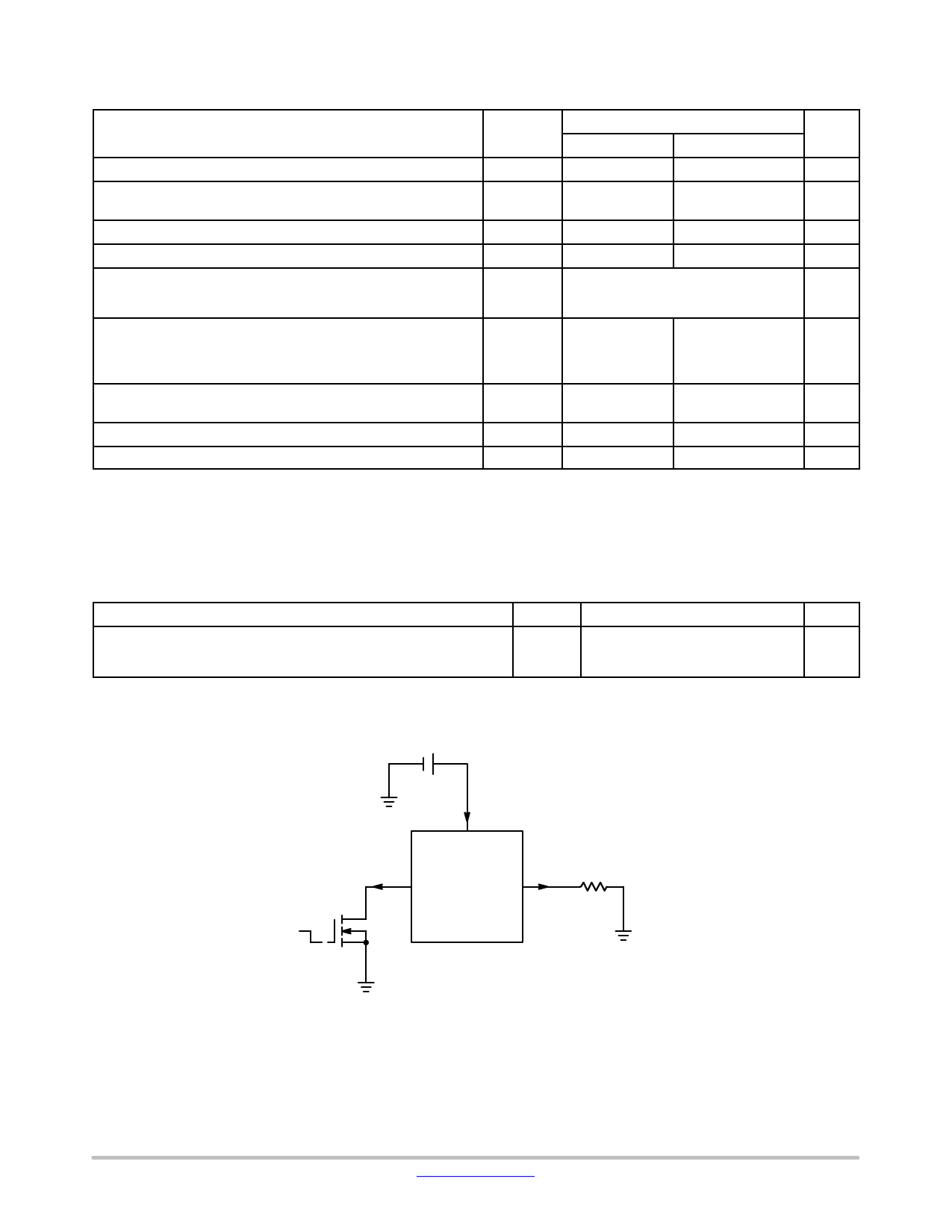
NCV8450
Figure 2. Applications Test Circuit
http://onsemi.com
3
Share Link: 