NCV8612 View Datasheet(PDF) - ON Semiconductor
Part Name
Description
Manufacturer
NCV8612
ON Semiconductor
NCV8612 Datasheet PDF : 26 Pages
| |||
NCV8612
CIRCUIT DESCRIPTION
Auto Switchover Circuitry
The auto switchover circuit is designed to insure
continuous operation of the device, automatically switching
the input voltage from the ASO_RAIL input, to the VIN−B
input, to the VIN−H input depending on conditions. The
primary input voltage pin is ASO_RAIL, which is driven
from the 8 V supply. When this voltage is present it will drive
the output voltages. Regardless of whether the 8 V supply is
available, the reference and core functions of the device will
be driven by the higher of VIN−B and VIN−H. The
switchover control circuitry will be powered solely by the
8 V supply, via VIN−A.
When the 8 V supply is not present, the gates of the 2
P−FET switches will be pulled to ground, turning the
switches on. In this condition, the VIN−B and VIN−H
voltages will be diode or’ed, with the higher voltage
powering the chip. The VIN−H voltage will be one diode
lower than the VIN−B voltage, thereby forcing the VIN−B
voltage to be dominant supply.
In the event that both the 8 V supply and the VIN−B supply
are not present, the VIN−H supply will be powering the
device. The VIN−H supply is then fed from a recommended
1000 mF cap. The duration of VIN−H supply is dependent on
output current. It is intended as protection against temporary
loss of battery conditions.
In the event of a double battery, or prolonged high voltage
condition on the battery line, a bleed transistor has been
included on the VIN−H line. With the large hold−up cap on
VIN−H, the voltage on that pin has the potential to remain
in an elevated position for an extended period of time. The
main result of this condition would be an
Overvoltage Shutdown of the device. In order to avoid this
condition, a transistor that is connected to the
Overvoltage Shutdown signal is tied to the VIN−H line. This
transistor will become active in a high voltage event,
allowing the hold−up cap to discharge the excess voltage in
a timely manner.
In the Block Diagram, Figure 1, CASO_RAIL is listed as a
1 mF capacitor. It is required for proper operation of the
device that CASO_RAIL is no larger than 1 mF.
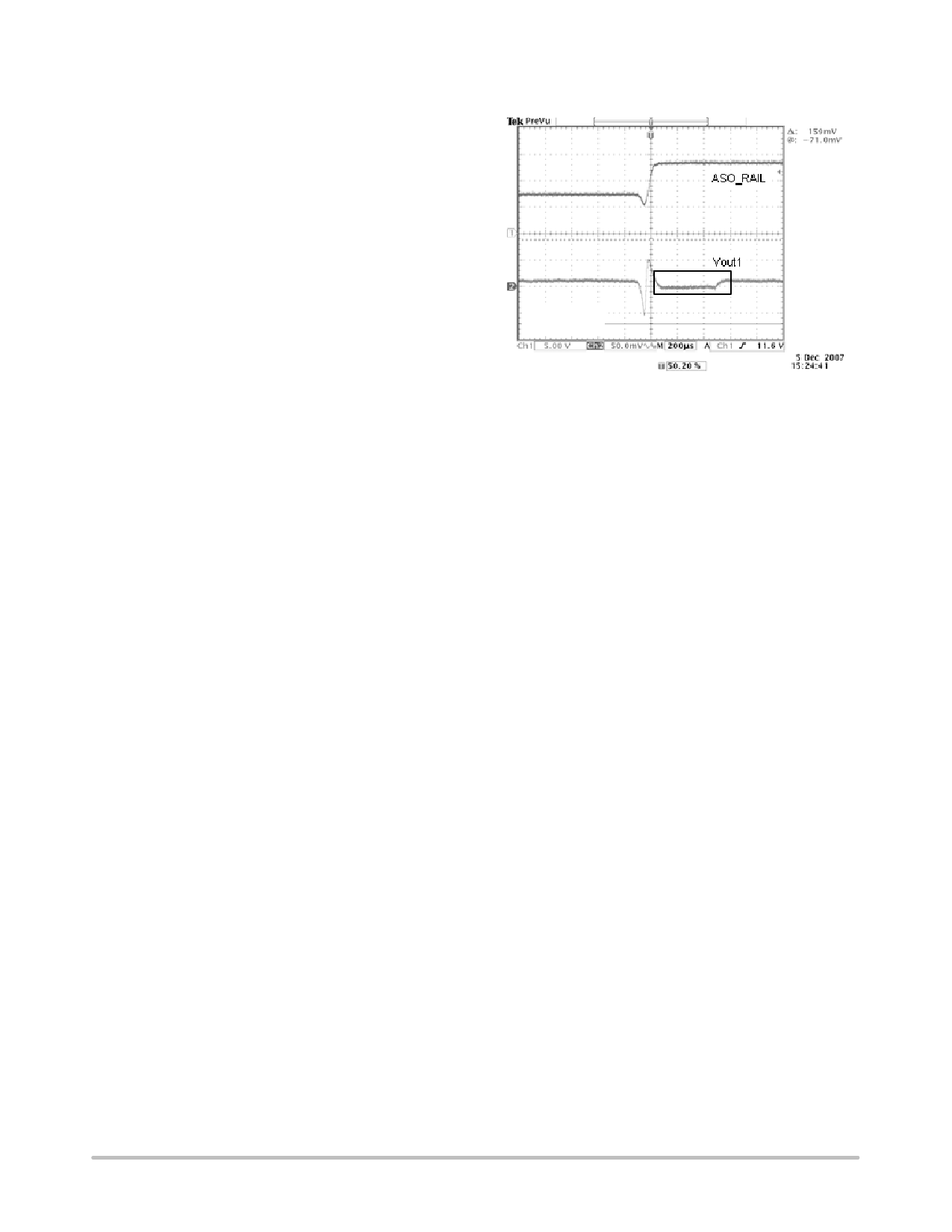
During a switchover event, a timer in the output stages
prepares the regulator in anticipation of change in input
voltage. The event results in a hitch in the output waveforms,
as can be seen in Figure 3.
IOUT = 120 mA
COUT = 47 mF
Figure 3. VOUTX Response to ASO Switchover Event
VIN−B/VIN−H Minimum Operating Voltage
The internal reference and core functions are powered by
either the VIN−B or VIN−H supply. The higher of the two
voltages will dominate and power the reference. This
provides quick circuit response on start−up, as well as a
stable reference voltage. Since the VIN−B voltage will come
up much more quickly than the VIN−H voltage, initially, the
VIN−B voltage will be running the reference. In the case of
any transient drops on VIN−B, the VIN−H supply, with its
large hold−up capacitor, will then be the dominant voltage,
and will be powering the reference.
For proper operation of the device, VIN−B or VIN−H
must be at least 4.5 V. Below that voltage the reference will
not operate properly, leading to incorrect functioning by the
device. VIN−B or VIN−H must be greater than 4.5 V
regardless of the voltage on the VIN−A pin.
Enable Function
The NCV8612 is equipped with an Enable input. By
keeping the Enable voltage below 0.8 V, the three outputs
will be held low. By increasing the Enable pin voltage above
2.0 V, the three outputs will be enabled to their regulated
output voltage.
Internal Soft−Start
The NCV8612 is equipped with an internal soft−start
function. This function is included to limit inrush currents
http://onsemi.com
9
Share Link: 