BF1102 View Datasheet(PDF) - Philips Electronics
Part Name
Description
Manufacturer
BF1102 Datasheet PDF : 16 Pages
| |||
Philips Semiconductors
Dual N-channel dual gate MOS-FETs
LIMITING VALUES
In accordance with the Absolute Maximum Rating System (IEC 60134).
SYMBOL
PARAMETER
CONDITIONS
Per MOS-FET unless otherwise specified
VDS
drain-source voltage
ID
drain current (DC)
IG1
gate 1 current
IG2
gate 2 current
Ptot
total power dissipation
Tstg
storage temperature
Tj
operating junction temperature
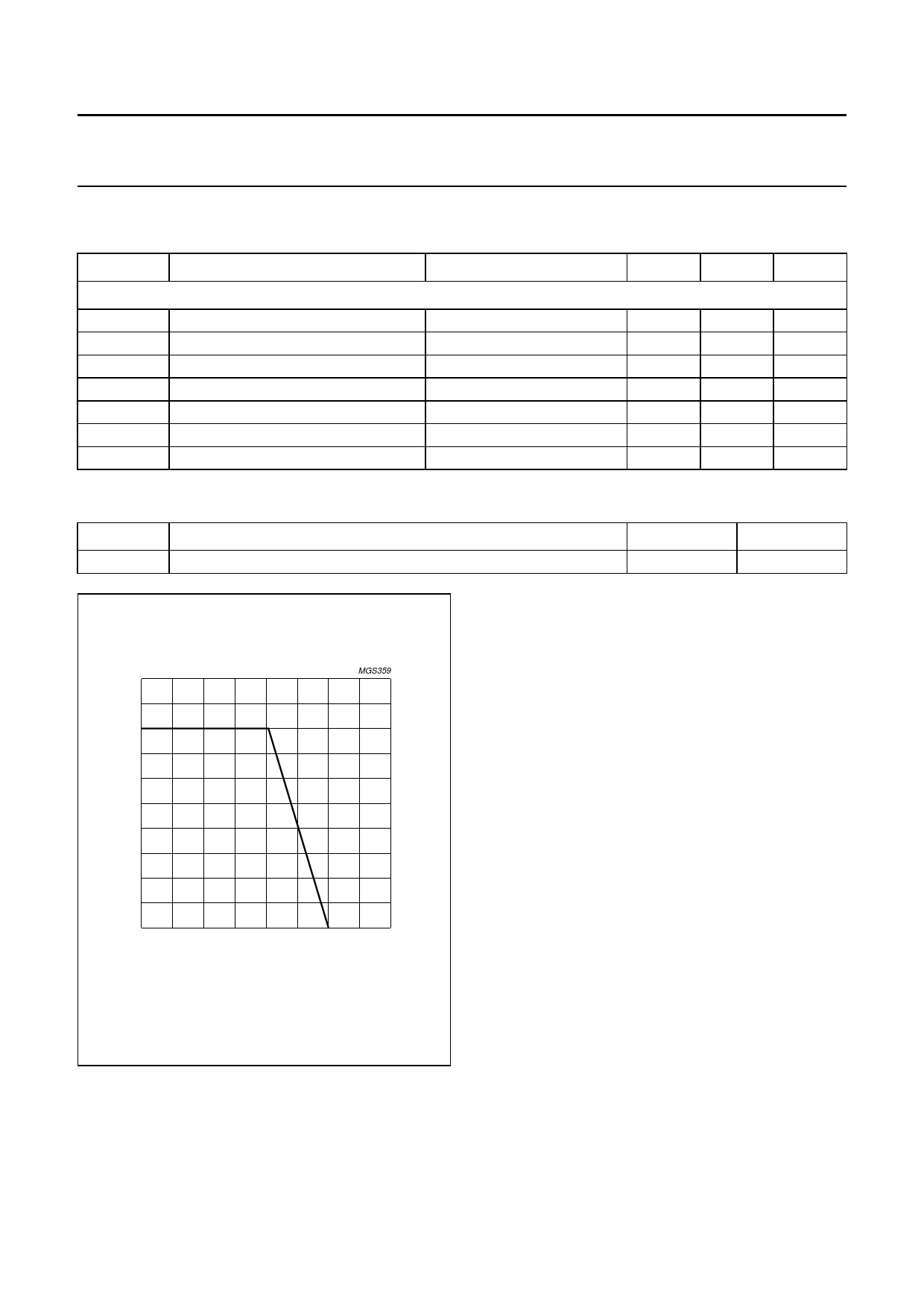
Ts ≤ 102 °C
THERMAL CHARACTERISTICS
SYMBOL
PARAMETER
Rth j-s
thermal resistance from junction to soldering point
Product specification
BF1102; BF1102R
MIN.
MAX.
UNIT
−
7
V
−
40
mA
−
±10
mA
−
±10
mA
−
200
mW
−65
+150
°C
−
150
°C
VALUE
240
UNIT
K/W
handboPot2ko,5th0alfpage
(mW)
200
150
100
50
0
0
50
MGS359
100
150
200
Ts (°C)
Fig.2 Power derating curve.
2000 Apr 11
3
Share Link: 