SL432XSF View Datasheet(PDF) - AUK -> KODENSHI CORP
Part Name
Description
Manufacturer
SL432XSF Datasheet PDF : 5 Pages
| |||
SL432xSF
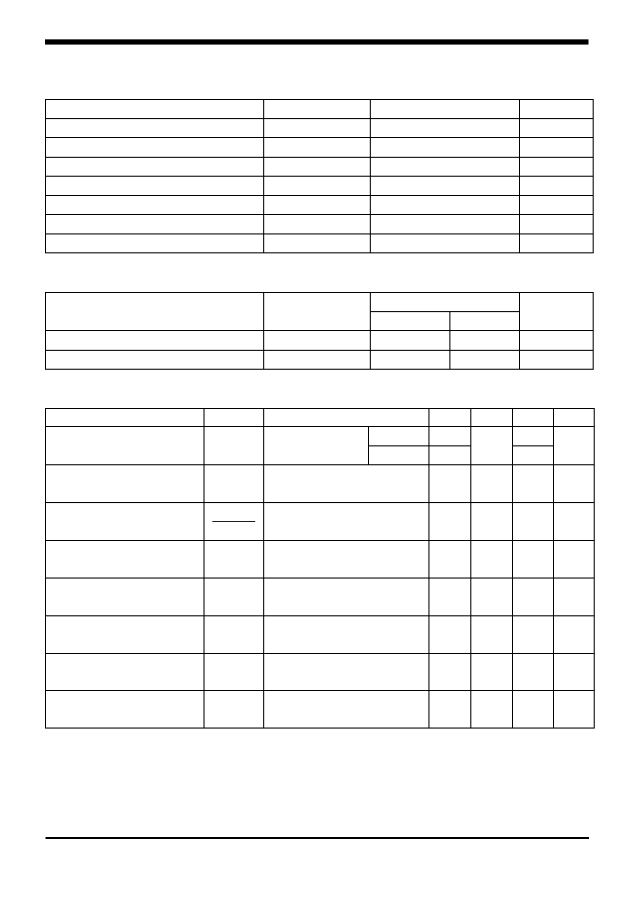
Absolute maximum ratings
Characteristic
Symbol
Rating
Cathode to Anode voltage
VKA
18
Cathode Current
IK
30
Reference Input Current
Power Dissipation
Iref
3
PD*
350
Junction Temperature
TJ
150
Operating Temperature Range
Topr
-40 ~ +85
Storage Temperature Range
Tstg
-55 ~ +150
* With PCB(8×8mm copper area) at glass epoxy board(t=1.7mm, area : 20×20mm)
Recommended operating conditions
Characteristic
Symbol
Rating
Min.
Max.
Cathode voltage
VKA
Vref
16
Cathode current
IK
0.1
30
[Ta=25℃]
Unit
V
mA
mA
mW
℃
℃
℃
Unit
V
mA
Electrical Characteristics (Ta=25℃, unless otherwise noted.)
Characteristic
Symbol
Condition
Reference voltage (Fig.1)
Reference input voltage
deviation over temperature
(Fig.1, Note1,2)
Ratio of delta reference input
voltage to delta cathode
voltage (Fig.2)
Vref
∆Vref
∆Vref
∆VKA
VKA=Vref, IK=10mA
SL432ASF
SL432SF
VKA=Vref, IK=10mA
@ -40˚C ≤ Ta ≤ 85˚C
IK=10mA
Vref ≤ VKA ≤ 16V
Reference current (Fig,2)
Iref
IK=10mA
R1=10KΩ, R2=∞
Reference input current
deviation over temperature
(Fig.2, Note 1,2)
∆Iref
IK=10mA
R1=10KΩ, R2=∞
Minimum cathode current
for Regulation
IK(MIN)
VKA=Vref
Min.
1.228
1.215
-
-
-
-
-
Typ.
1.240
Max.
1.252
1.265
10
20
-1.0 -2.7
0.15 0.3
0.04 0.08
55
80
Unit
V
mV
mV/V
µΑ
µΑ
µΑ
Off-state cathode current
(Fig.3)
IK(off)
VKA=16V, Vref=0V
-
5
50
nA
Dynamic impedance
(Fig.1, Note3)
ZKA
VKA=Vref, f ≤ 1.0KHz
0.1mA ≤ IK ≤ 30mA
-
0.25 0.4
Ω
KSI-2015-005
2
Share Link: 