ST890D View Datasheet(PDF) - STMicroelectronics
Part Name
Description
Manufacturer
ST890D Datasheet PDF : 17 Pages
| |||
Device summary
ST890B, ST890C, ST890D
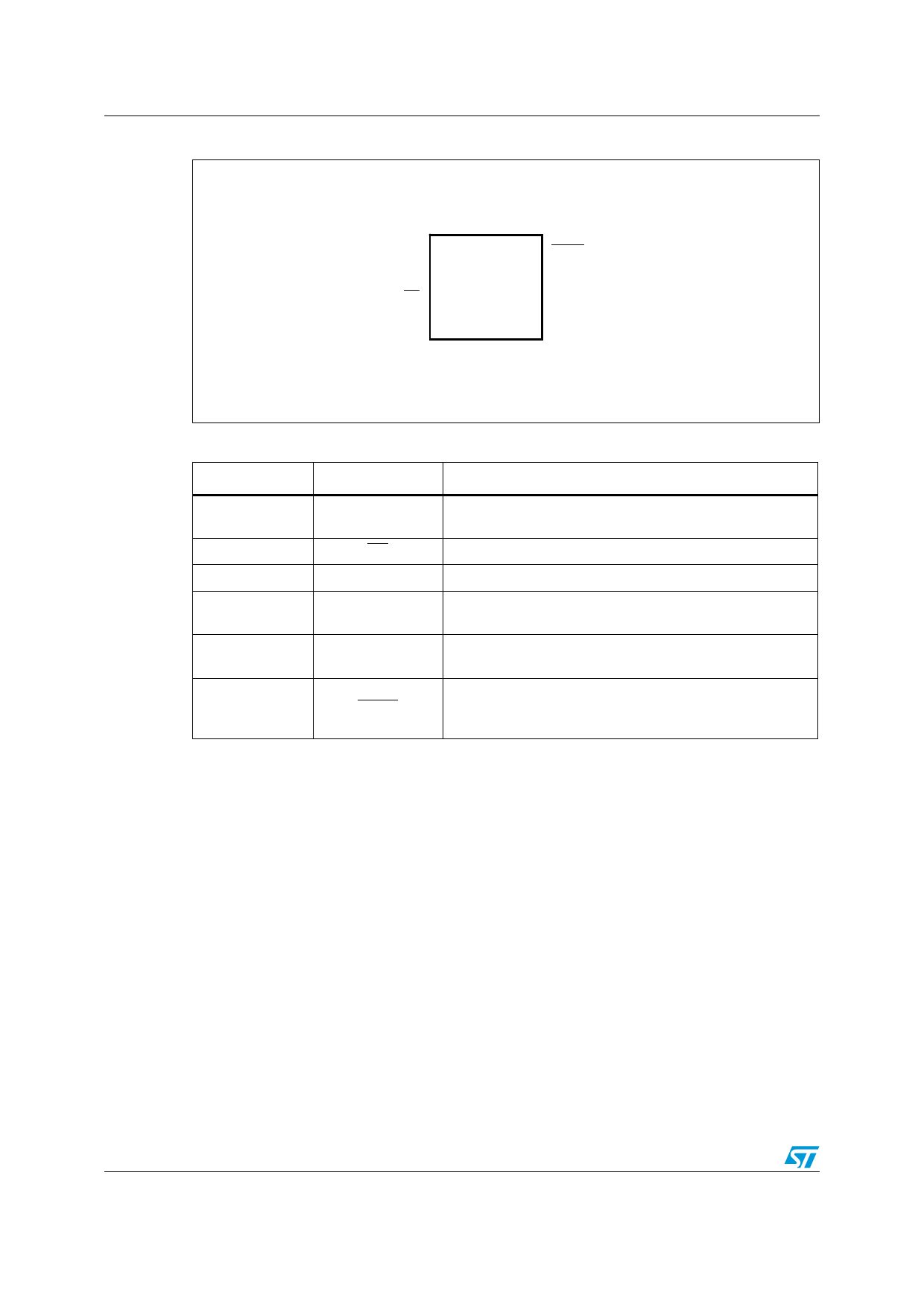
Figure 2. DFN8L (3 x 3 mm) pin connection (top view)
IN 1
IN 2
ON 3
GND 4
8 FAULT
7 OUT
6 OUT
5 SET
CS00025
Table 3. DFN8L (3 x 3 mm) pin description
Pin N.
Symbol
Name and function
1, 2
IN
Input P-channel MOSFET source. Bypass IN with a 1 μF
capacitor to ground
3
ON
Active low switch ON input. A logic low turns the switch ON
4
GND
Ground
5
SET
Set current limit input. A resistor from SET to GND sets the
current limit for the switch.
6,7
OUT
Switch output. P-channel MOSFET drain. Bypass OUT with
a 0.1 μF capacitor to ground
Fault indicator output. This open drain output goes low
8
FAULT
when in current limit or when the die temperature exceeds
135 °C
4/17
Share Link: 