ST8009 View Datasheet(PDF) - Sitronix Technology Co., Ltd.
Part Name
Description
Manufacturer
ST8009 Datasheet PDF : 43 Pages
| |||
ST8009
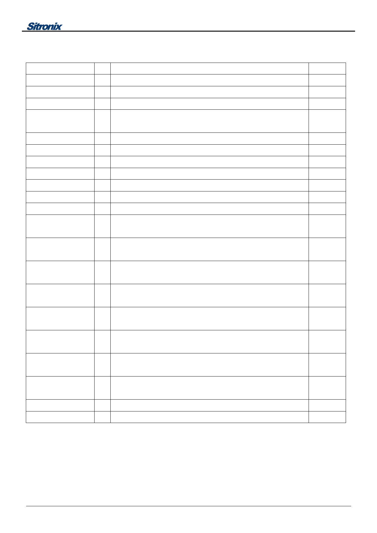
5. PIN DESCRIPTION
SYMBOL
CS0~CS95
V0~V4
VDD
EIO2, EIO1
DI0~DI3
XCK
XDISPOFF
LP1
LP2
FR
VSS
CAP1-
CAP1+
CAP2-
CAP2+
CAP3+
CAP4+
CAP5+
VOUT
SID
SCLK
I/O
DESCRIPTION
No of Num
O LCD drive output
96
P Power supply for LCD drive
5
P Power supply for logic system (+2.5 to +5.5 V)
1
Input/output for chip selection at segment mode and FLM input output
I/O
2
function at com/seg mix mode or common mode
I Display data input at segment mode
4
I Clock input for taking display data at segment mode
1
I Control input for output of ground level
1
I Latch pulse input for display data at segment mode
1
I Shift clock input for shift register at common mode
1
I AC-converting signal input for LCD drive waveform
1
P Ground (0 V)
1
DC/DC voltage converter. Connect a capacitor between this terminal
O
1
and the CAP2- terminal.
DC/DC voltage converter. Connect a capacitor between this terminal
O
1
and the CAP1- terminal.
DC/DC voltage converter. Connect a capacitor between this terminal
O
1
and the CAP2- terminal.
DC/DC voltage converter. Connect a capacitor between this terminal
O
1
and the CAP2- terminal.
DC/DC voltage converter. Connect a capacitor between this terminal
O
1
and the CAP1- terminal.
DC/DC voltage converter. Connect a capacitor between this terminal
O
1
and the CAP2- terminal.
DC/DC voltage converter. Connect a capacitor between this terminal
O
and the CAP1- terminal.
DC/DC voltage converter. Connect a capacitor between this terminal
O
1
and VSS.
I The command data. See Figure1
1
I The serial clock input. See Figure1
1
V1.1
5/43
2006/11/1
Share Link: 