STK16C88-3 View Datasheet(PDF) - Simtek Corporation
Part Name
Description
Manufacturer
STK16C88-3 Datasheet PDF : 13 Pages
| |||
STK16C88-3
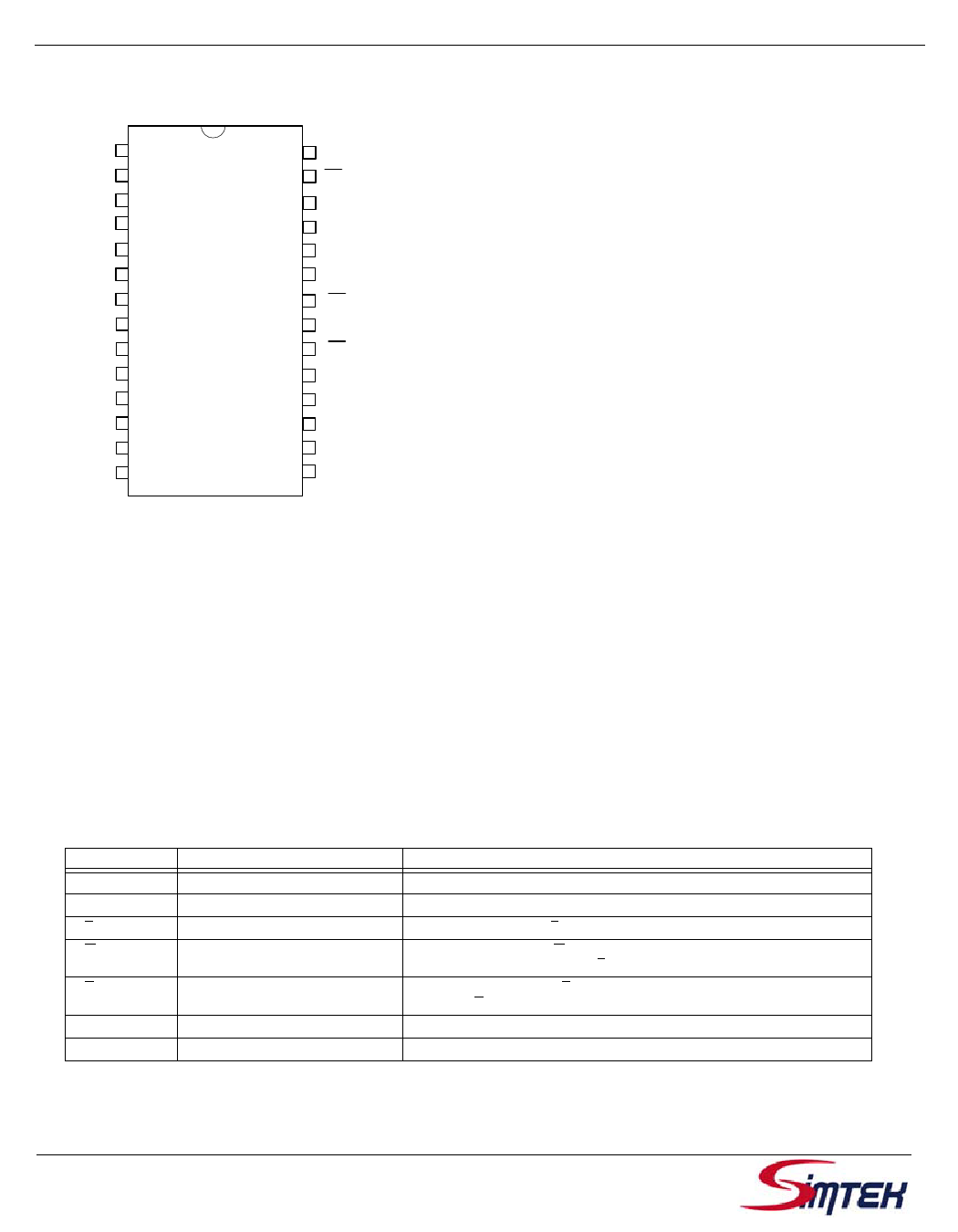
PIN CONFIGURATIONS
A14 1
A12 2
A7 3
A6 4
A5 5
A4 6
A3
7
A2 8
A1 9
A0 10
DQ0 11
DQ1 12
DQ2 13
VSS
14
(TOP)
28 VCC
27 W
26 A13
25 A8
24 A9
23 A11
22 G
21 A10
20 E
19 DQ7
18 DQ6
17 DQ5
16 DQ4
15 DQ3
28 Pin 600 mil PDIP
PIN DESCRIPTIONS
Pin Name
A14-A0
DQ7-DQ0
E
W
G
VCC
VSS
I/O
Input
I/O
Input
Input
Input
Power Supply
Power Supply
Description
Address: The 15 address inputs select one of 32,768 bytes in the nvSRAM array
Data: Bi-directional 8-bit data bus for accessing the nvSRAM
Chip Enable: The active low E input selects the device
Write Enable: The active low W enables data on the DQ pins to be written to the address
location latched by the falling edge of E
Output Enable: The active low G input enables the data output buffers during read cycles.
De-asserting G high caused the DQ pins to tri-state.
Power: 3.3V, ±0.3V
Ground
Document Control #ML0019 Rev 2.0
2
Jan, 2008
Share Link: 