TA8492PG(2004) View Datasheet(PDF) - Toshiba
Part Name
Description
Manufacturer
TA8492PG Datasheet PDF : 13 Pages
| |||
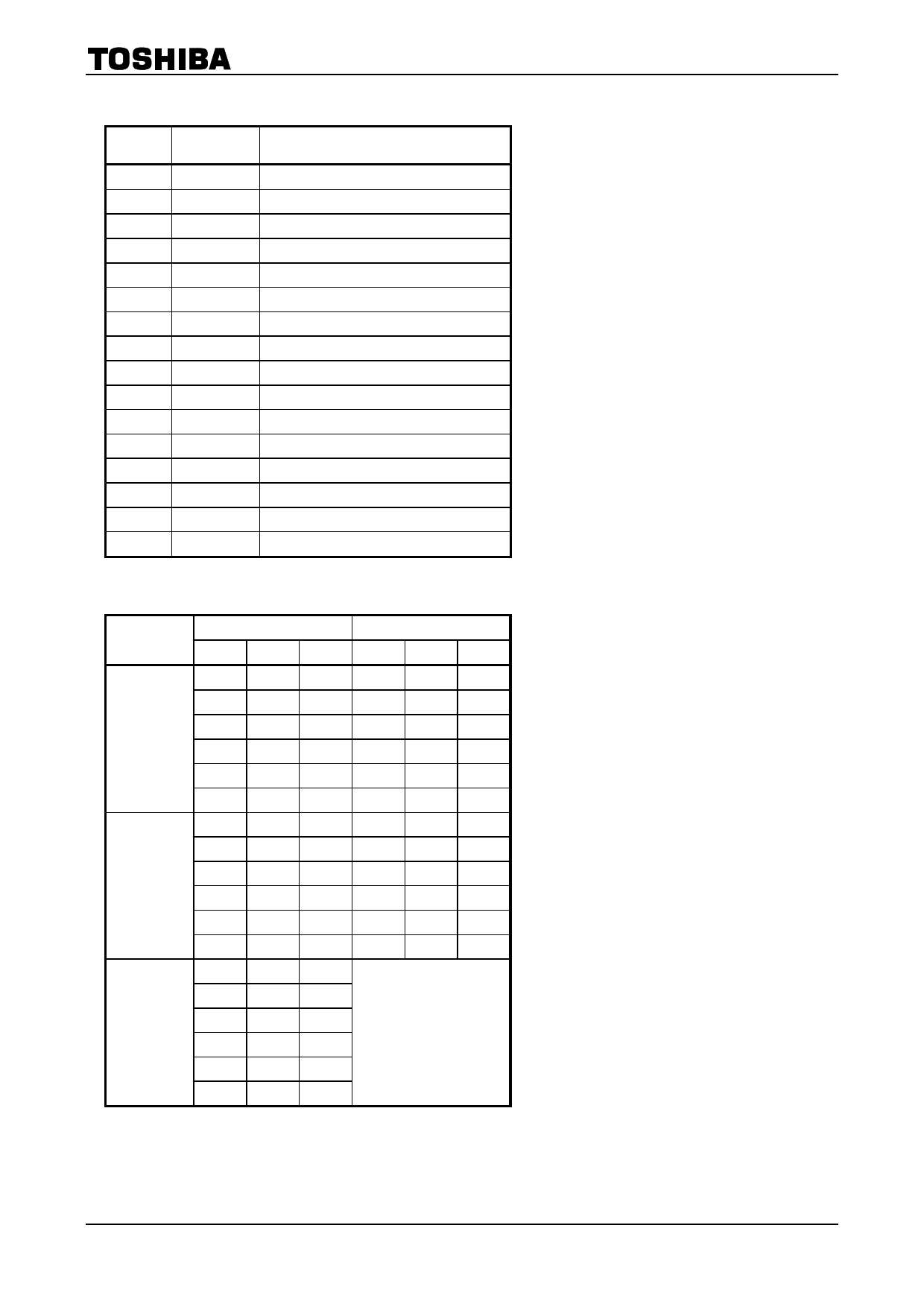
Pin Function
Pin No.
1
2
3
4
5
6
7
8
9
10
11
12
13
14
15
16
Symbol
Lc
La
3ST
GND
GND
Ha−
Ha+
Hc−
Hc+
Hb−
Hb+
GND
GND
VCC
Lb
VS
Function
c-phase drive output pin
a-phase drive output pin
Switching CW/CCW/Stop
⎯
⎯
a-phase negative hall signal input pin
a-phase positive hall signal input pin
c-phase negative hall signal input pin
c-phase positive hall signal input pin
b-phase negative hall signal input pin
b-phase positive hall signal input pin
⎯
⎯
Supply voltage pin for control circuits
b-phase drive output pin
Supply voltage pin for output circuit
Function
FRS
Forward
Reverse
Stop
Hall Input
Ha
Hb
Hc
1
0
1
1
0
0
1
1
0
0
1
0
0
1
1
0
0
1
1
0
1
1
0
0
1
1
0
0
1
0
0
1
1
0
0
1
1
0
1
1
0
0
1
1
0
0
1
0
0
1
1
0
0
1
Output
La
Lb
Lc
L
H
M
L
M
H
M
L
H
H
L
M
H
M
L
M
H
L
H
L
M
H
M
L
M
H
L
L
H
M
L
M
H
M
L
H
High Impedance
2
TA8492P/PG
2004-07-27
Share Link: 