TCET1113 View Datasheet(PDF) - Vishay Semiconductors
Part Name
Description
Manufacturer
TCET1113 Datasheet PDF : 9 Pages
| |||
VISHAY
Switching Characteristics
Parameter
Delay time (see figure 3)
Rise time (see figure 3)
Turn-on time (see figure 3)
Storage time (see figure 3)
Fall time (see figure 3)
Turn-off time (see figure 3)
Turn-on time see figure 4)
Turn-off time see figure 4)
Test condition
VS = 5 V, IC = 2 mA, RL = 100 Ω
VS = 5 V, IC = 2 mA, RL = 100 Ω
VS = 5 V, IC = 2 mA, RL = 100 Ω
VS = 5 V, IC = 2 mA, RL = 100 Ω
VS = 5 V, IC = 2 mA, RL = 100 Ω
VS = 5 V, IC = 2 mA, RL = 100 Ω
VS = 5 V, IF = 10 mA, RL = 1 kΩ
VS = 5 V, IF = 10 mA, RL = 1 kΩ
TCET111.(G)
Vishay Semiconductors
Symbol
Typ.
Unit
td
3.0
µs
tr
3.0
µs
ton
6.0
µs
ts
0.3
µs
tf
4.7
µs
toff
5.0
µs
ton
9.0
µs
toff
10.0
µs
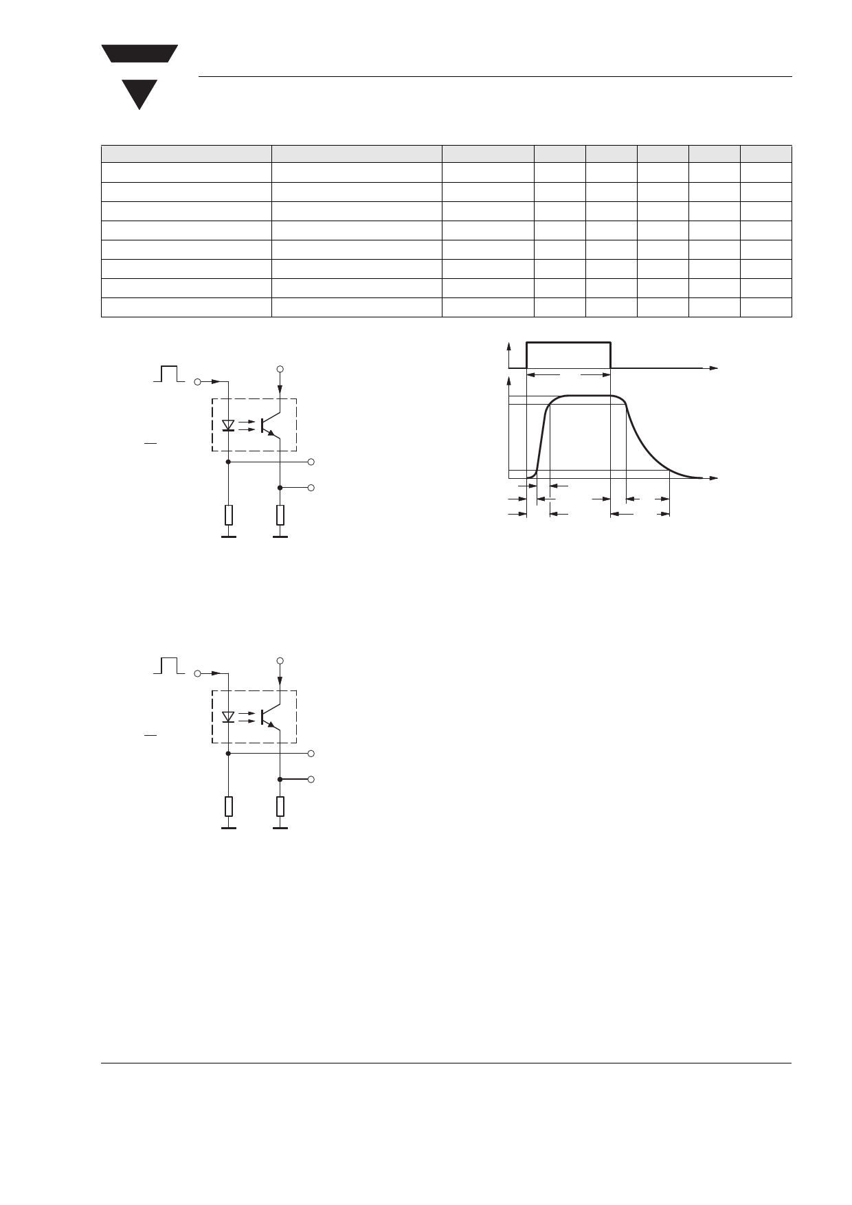
IF IF
0
RG = 50 W
tp = 0.01
T
tp = 50 Ps
50 W
+5V
IC = 2 mA; adjusted through
input amplitude
100 W
Channel I
Channel II
Oscilloscope
RL = 1 MW
CL = 20 pF
95 10804
Figure 3. Test circuit, non-saturated operation
IF
0
IC
tp
100%
90%
96 11698
t
10%
0
tp
td
tr
ton (= td + tr)
tr
td
ton
pulse duration
delay time
rise time
turn-on time
ts
tf
toff
ts
tf
toff (= ts + tf)
t
storage time
fall time
turn-off time
Figure 5. Switching times
IF IF = 10 mA
0
+5V
IC
RG = 50 W
tp = 0.01
T
tp = 50 Ps
50 W
Channel I
1 kW
Channel II
95 10843
Oscilloscope
RL t 1 MW
CL d 20 pF
Figure 4. Test circuit, saturated operation
Document Number 83546
Rev. A3, 18-Mar-03
www.vishay.com
5
Share Link: 