TDA8716 View Datasheet(PDF) - Philips Electronics
Part Name
Description
Manufacturer
TDA8716 Datasheet PDF : 21 Pages
| |||
Philips Semiconductors
8-bit high-speed analog-to-digital converter
Product specification
TDA8716
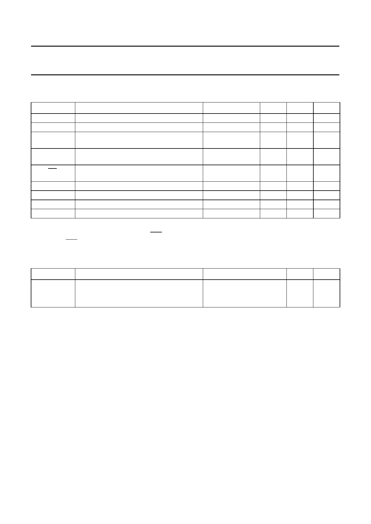
LIMITING VALUES
In accordance with the Absolute Maximum Rating System (IEC 134).
SYMBOL
VEEA
VEED1,VEED2
VEEA − VEED1;
VEEA − VEED2
VI
PARAMETER
analog supply voltage
digital supply voltage
supply voltage differences
input voltage
VCLK; CLK(p-p)
IO
Tstg
Tamb
Tj
input voltage for differential clock drive
(peak-to-peak value)
output current (each output stage)
storage temperature
operating ambient temperature
junction temperature
CONDITIONS
MIN.
−7.0
−7.0
−1
MAX.
+0.3
+0.3
+1
UNIT
V
V
V
referenced to
AGND
note 1
VEEA
0
V
−
2.0
V
−
10
mA
−55
+150 °C
0
+70
°C
−
+150 °C
Note
1. The circuit has two clock inputs: CLK and CLK. Sampling takes place on the rising edge of the clock input signal:
CLK and CLK are two's complementary ECL signals.
THERMAL CHARACTERISTICS
SYMBOL
Rth j-a
PARAMETER
from junction to ambient
SOT101
SOT287 (see Fig.4)
CONDITIONS
in free air
VALUE UNIT
35
K/W
65
K/W
HANDLING
Inputs and outputs are protected against electrostatic discharge in normal handling. However, to be totally safe, it is
desirable to take normal precautions appropriate to handling integrated circuits.
1996 Aug 26
6
Share Link: 