TGS2351 View Datasheet(PDF) - TriQuint Semiconductor
Part Name
Description
Manufacturer
TGS2351 Datasheet PDF : 11 Pages
| |||
TGS2351
DC – 6 GHz High Power SPDT Switch
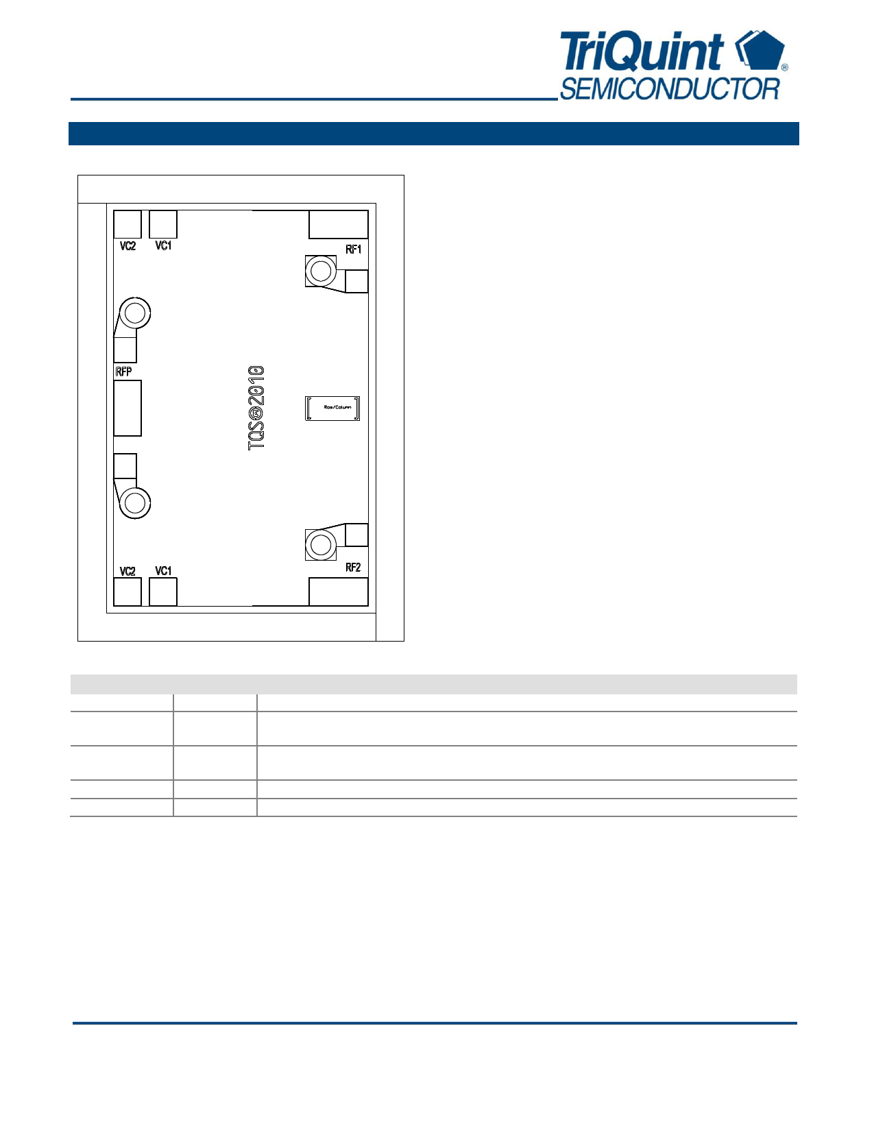
Bond Pad Description
23
4
1
76
5
Bond Pad
1
2, 7
3, 6
4
5
Symbol
RF In
Vc2
Vc1
RF Out1
RF Out2
Description
Input, matched to 50 ohms, DC coupled
Control voltage #2; can be biased from either side (bond pad 2 or bond pad 7), and non-
biased bond pad can be left opened; see Application Circuit on page 6 as an example
Control voltage #1; can be biased from either side (bond pad 3 or bond pad 6), and non-
biased bond pad can be left opened; see Application Circuit on page 6 as an example
Output #1, matched to 50 ohms, DC coupled
Output #2, matched to 50 ohms, DC coupled
Data Sheet: Rev B 06/20/12
© 2012 TriQuint Semiconductor, Inc.
- 7 of 11 -
Disclaimer: Subject to change without notice
Connecting the Digital World to the Global Network®
Share Link: 