NJVMJD45H11RLG(2012) View Datasheet(PDF) - ON Semiconductor
Part Name
Description
Manufacturer
NJVMJD45H11RLG Datasheet PDF : 9 Pages
| |||
MJD44H11, NJVMJD44H11 (NPN), MJD45H11, NJVMJD45H11 (PNP)
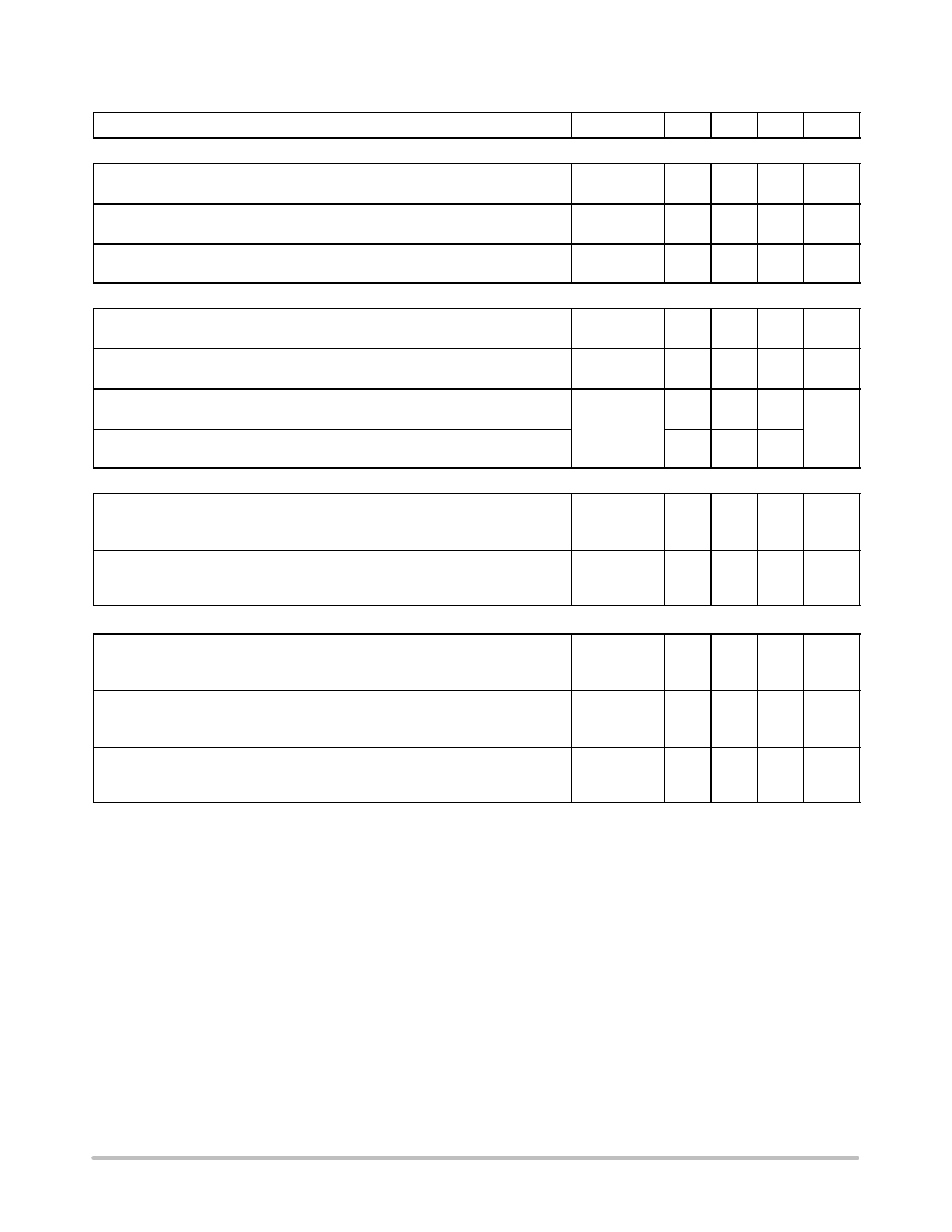
MAXIMUM RATINGS (TA = 25_C, common for NPN and PNP, minus sign, “−”, for PNP omitted, unless otherwise noted)
Rating
Symbol
Max
Unit
Collector−Emitter Voltage
Emitter−Base Voltage
Collector Current − Continuous
− Peak
VCEO
80
Vdc
VEB
5
Vdc
IC
8
Adc
16
Total Power Dissipation
@ TC = 25°C
Derate above 25°C
PD
W
20
0.16
W/°C
Total Power Dissipation (Note 1)
@ TA = 25°C
Derate above 25°C
PD
W
1.75
0.014
W/°C
Operating and Storage Junction
Temperature Range
TJ, Tstg
−55 to +150
°C
Stresses exceeding Maximum Ratings may damage the device. Maximum Ratings are stress ratings only. Functional operation above the
Recommended Operating Conditions is not implied. Extended exposure to stresses above the Recommended Operating Conditions may affect
device reliability.
THERMAL CHARACTERISTICS
Characteristic
Symbol
Max
Thermal Resistance, Junction−to−Case
Thermal Resistance, Junction−to−Ambient (Note 1)
Lead Temperature for Soldering
RqJC
RqJA
TL
6.25
71.4
260
1. These ratings are applicable when surface mounted on the minimum pad sizes recommended.
Unit
°C/W
°C/W
°C
http://onsemi.com
2
Share Link: 