UC3842B View Datasheet(PDF) - Unisonic Technologies
Part Name
Description
Manufacturer
UC3842B Datasheet PDF : 11 Pages
| |||
UC3842B/3843B
LINEAR INTEGRATED CIRCUIT
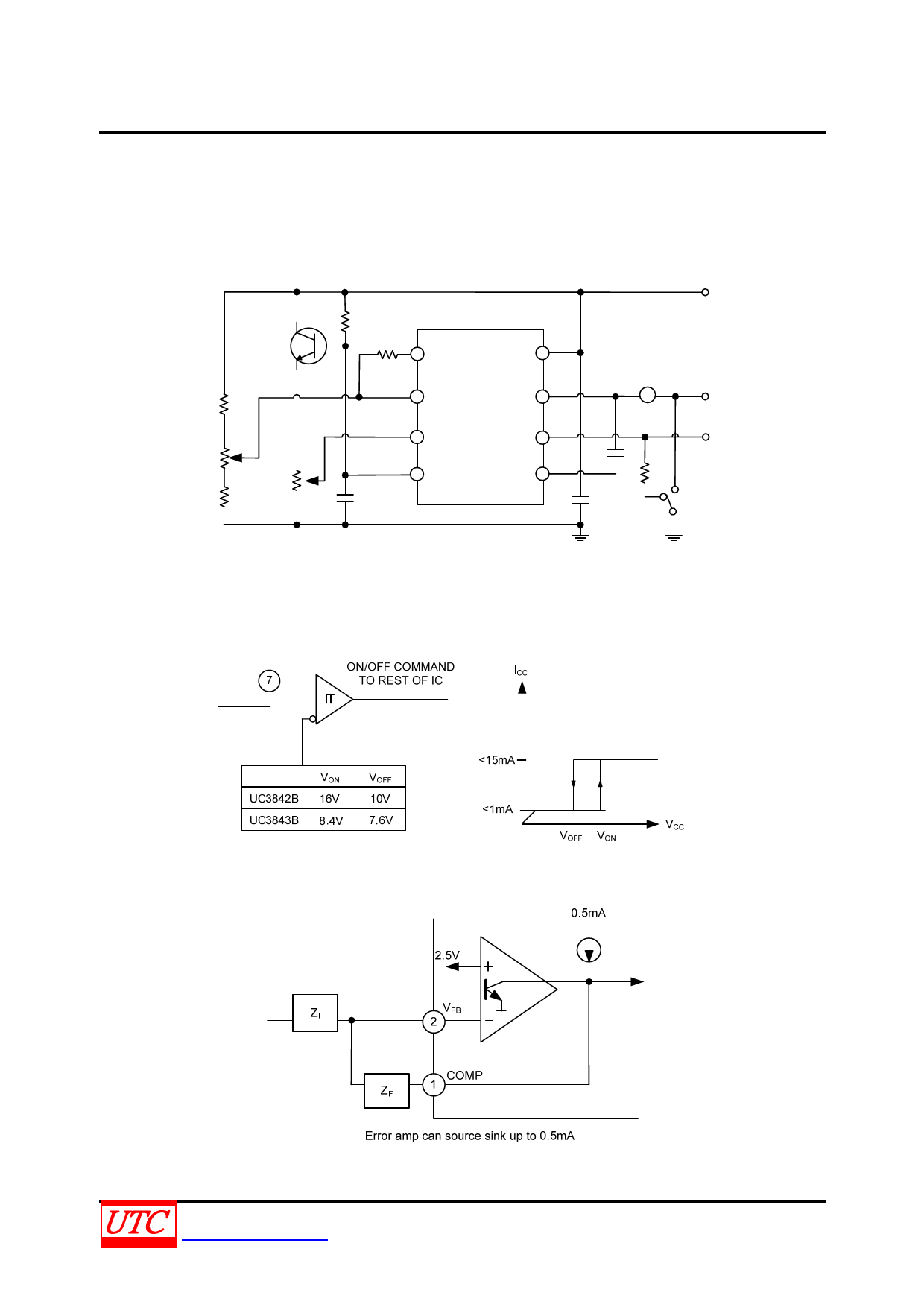
TYPICAL APPLICATION CIRCUIT
Open Loop Test Circuit
All of the parameters are not all tested in production, although been guaranteed. The timing and bypass capacitors
must be connected to pin 5 in a single point ground very closely. To sample the oscillator waveform, the transistor
and 5kΩ potentiometer are used, and also can apply an adjustable ramp to ISENSE pin.
4.7K
2N
2222
UTC
RT
UC3842B/3843B
1 COMP
100K
VREF 8
2 VFB
VC 7
VREF
A
V1
E/A 1K
ADJUST
ISENSE 5K
ADJUST
4.7K
CT
3 ISENSE
OUTPUT 6
4 RT/CT
GND 5
0.1
0.1
OUTPUT
1K/1W
Under Voltage Lockout
Under-Voltage Lock-Out: the output driver is biased to a high impedance state. To prevent activating the power
switch with output leakage current, pin 6 should be shunted to ground with a bleeder resistor.
Error Amp Configuration
UNISONIC TECHNOLOGIES CO., LTD
www.unisonic.com.tw
6 of 11
QW-R103-012.D
Share Link: 