UC3842G(2007) View Datasheet(PDF) - Unisonic Technologies
Part Name
Description
Manufacturer
UC3842G Datasheet PDF : 8 Pages
| |||
UC3842G
OPEN-LOOP TEST CIRCUIT
LINEAR INTEGRATED CIRCUIT
Ra
VIN
100k
or
VCOMP
Rb
100k
VFB
1
10p
2
COMP
FB
Vpwl
adjust 5K
CT
3.3n
3 CS
4 CT
VREF 8
VCC 7
VCC
Output 6
GND 5
CIN
470μ
High peak current associated with capacity loads necessitate careful grounding techniques. Timing and bypass
capacitors should be connected close to pin5 in single point GND.
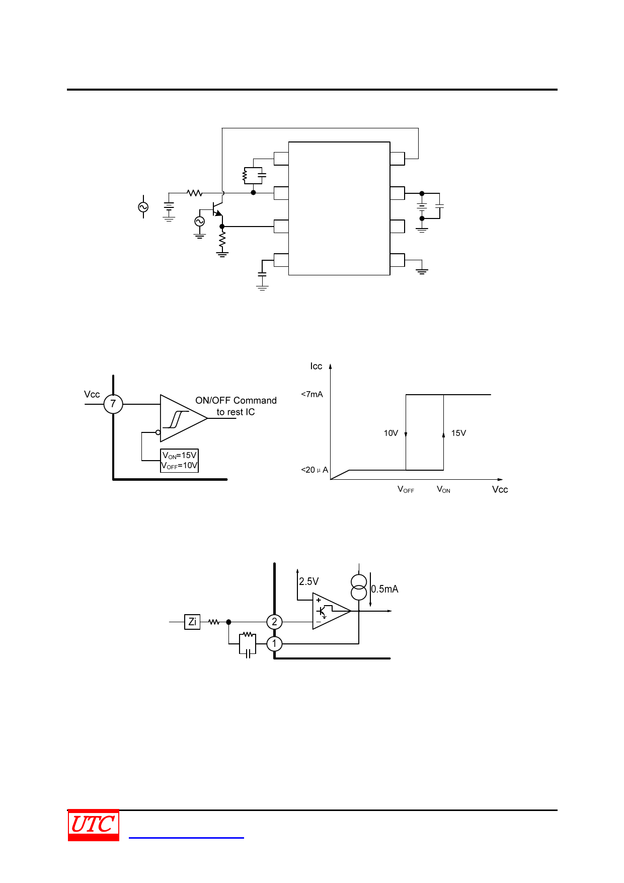
UNDER-VOLTAGE LOCKOUT
During Under-Voltage Lockout, the output driver is biased to a high impedance state. Pin6 should be shunt to
GND with a bleeder resistor to prevent activing the power switch with output leakage currents.
ERROR AMPLIFIER CONFIGURATION
Error amplifier can source or sink up to 0.5mA
UNISONIC TECHNOLOGIES CO., LTD
www.unisonic.com.tw
6 of 8
QW-R103-036,A
Share Link: 