WM8150CDS/R View Datasheet(PDF) - Wolfson Microelectronics plc
Part Name
Description
Manufacturer
WM8150CDS/R
Wolfson Microelectronics plc
WM8150CDS/R Datasheet PDF : 26 Pages
| |||
Production Data
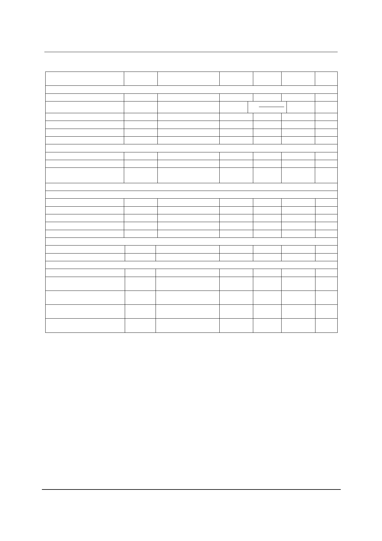
WM8150
Test Conditions
AVDD = DVDD1 = 5.0V, DVDD2 = 3.3V, AGND = DGND = 0V, TA = 25°C, MCLK = 16MHz unless otherwise stated.
PARAMETER
SYMBOL
TEST
CONDITIONS
MIN
TYP
MAX
Programmable Gain Amplifier
Resolution
Gain equation
8
0.78 + PGA[7 : 0]× 7.57
255
Max gain
Min gain
Gain error
GMAX
GMIN
6.8
8.35
8.7
0.75
0.78
0.82
1
2
Internal channel offset
VOFF
10
Analogue to Digital Converter
Resolution
12
Maximum Speed
8
Full-scale input range
VFS
2.5
(2*(VRT-VRB))
DIGITAL SPECIFICATIONS
Digital Inputs
High level input voltage
VIH
Low level input voltage
VIL
High level input current
IIH
Low level input current
IIL
Input capacitance
CI
Digital Outputs
0.8 ∗ DVDD2
0.2 ∗ DVDD2
1
1
5
High level output voltage
VOH
IOH = 1mA
DVDD2 - 0.5
Low level output voltage
VOL
IOL = 1mA
0.5
Supply Currents
Total supply current − active
35
45
Total analogue AVDD, supply
current − active
IAVDD
30
40
Total digital core, DVDD1,
supply current − active
IDVDD1
1.7
2
Digital I/O supply current,
DVDD2 − active (see note 3)
Supply current − full power down
mode
IDVDD2
4
5
300
400
Notes:
3.
Digital I/O supply current depends on the capacitive load attached to the pin. The Digital I/O supply current is
measured with approximately 50pF attached to the pin.
UNIT
bits
V/V
V/V
V/V
%
mV
bits
MSPS
V
V
V
µA
µA
pF
V
V
mA
mA
mA
mA
µA
w
PD Rev 4.1 February 2005
7
Share Link: 