2SB1188T100P View Datasheet(PDF) - ROHM Semiconductor
Part Name
Description
Manufacturer
2SB1188T100P Datasheet PDF : 3 Pages
| |||
Transistors
2SB1188 / 2SB1182 / 2SB1240
!Electrical characteristics (Ta=25°C)
Parameter
Symbol Min. Typ. Max. Unit
Conditions
Collector-base breakdown voltage BVCBO −40
−
−
V IC=−50µA
Collector-emitter breakdown voltage BVCEO −32
−
−
V IC=−1mA
Emitter-base breakdown voltage
BVEBO
−5
−
−
V IE=−50µA
Collector cutoff current
ICBO
−
−
−1
µA VCB=−20V
Emitter cutoff current
IEBO
−
−
−1
µA VEB=−4V
Collector-emitter saturation voltage
VCE(sat)
−
−0.5 −0.8
V
IC/IB=−2A/−0.2A
∗
DC current transfer ratio
hFE
82
−
390
− VCE=−3V, IC=−0.5A
∗
Transition frequency
fT
−
100
− MHz VCE=−5V, IE=0.5A, f=30MHz
Output capacitance
∗ Measured using pulse current.
Cob
−
50
−
pF VCB=−10V, IE=0A, f=1MHz
!Packaging specifications and hFE
Type
2SB1188
2SB1182
2SB1240
Package
Code
hFE Basic ordering unit (pieces)
PQR
PQR
PQR
T100
1000
−
−
Taping
TL
2500
−
−
TV2
2500
−
−
hFE values are classified as follows :
Item
P
Q
hFE
82~180 120~270
R
180~390
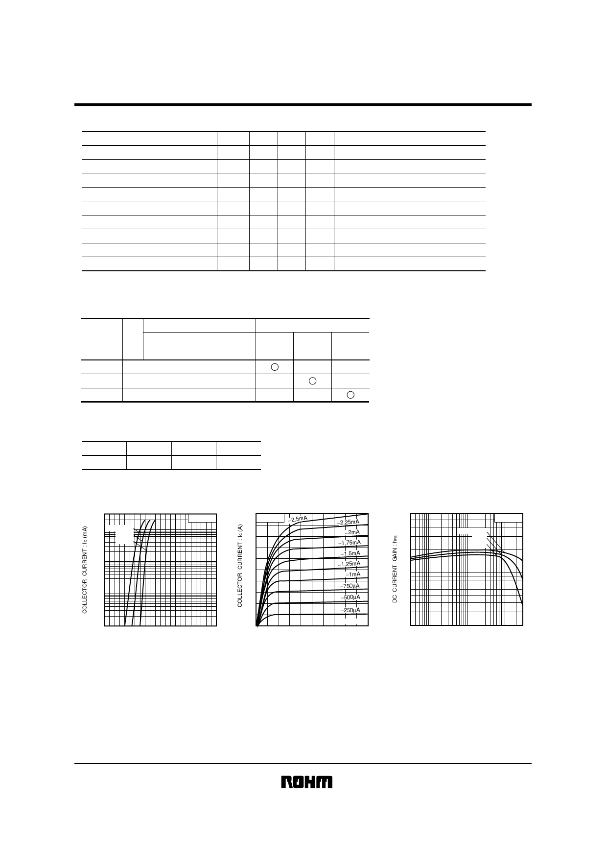
!Electrical characteristic curves
−1000 Ta=100°C
−500
25°C
−40°C
−200
−100
−50
VCE=−3V
−20
−10
−5
−2
−1
0 −0.2 −0.4 −0.6 −0.8 −1.0 −1.2 −1.4 −1.6 −1.8 −2.0 −2.2
BASE TO EMITTER VOLTAGE : VBE (V)
Fig.1 Grounded emitter propagation
characteristics
−0.5
Ta=25°C −2.5mA
−0.4
−0.3
−0.2
−2.25mA
−2mA
−1.75mA
−1.5mA
−1.25mA
−1mA
−750µA
−500µA
−0.1
−250µA
0
IB=0A
0
−0.4 −0.8 −1.2 −1.6 −2
COLLECTOR TO EMITTER VOLTAGE : VCE (V)
Fig.2 Grounded emitter output
characteristics
500
Ta=25°C
VCE=−6V
−3V
−1V
200
100
50
20 −5 −10 −20 −50 −100 −200 −500 −1000 −2000
COLLECTOR CURRENT : IC (mA)
Fig.3 DC current gain vs.
collector current ( Ι )
Share Link: 