BF620 View Datasheet(PDF) - Philips Electronics
Part Name
Description
Manufacturer
BF620 Datasheet PDF : 8 Pages
| |||
Philips Semiconductors
NPN high-voltage transistors
Product specification
BF620; BF622
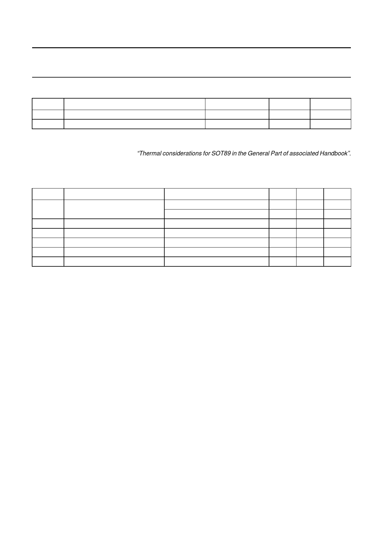
THERMAL CHARACTERISTICS
SYMBOL
PARAMETER
CONDITIONS
VALUE
UNIT
Rth j-a
Rth j-s
thermal resistance from junction to ambient
note 1
thermal resistance from junction to soldering point
100
K/W
20
K/W
Note
1. Device mounted on a printed-circuit board, single-sided copper, tinplated, mounting pad for collector 6 cm2.
For other mounting conditions, see “Thermal considerations for SOT89 in the General Part of associated Handbook”.
CHARACTERISTICS
Tj = 25 °C unless otherwise specified.
SYMBOL
PARAMETER
CONDITIONS
MIN.
ICBO
IEBO
hFE
VCEsat
Cre
fT
collector cut-off current
emitter cut-off current
DC current gain
collector-emitter saturation voltage
feedback capacitance
transition frequency
IE = 0; VCB = 200 V
−
IE = 0; VCB = 200 V; Tj = 150 °C
−
IC = 0; VEB = 5 V
−
IC = 25 mA; VCE = 20 V
50
IC = 30 mA; IB = 5 mA
−
IC = ic = 0; VCE = 30 V; f = 1 MHz
−
IC = 10 mA; VCE = 10 V; f = 100 MHz 60
MAX.
10
10
50
−
600
1.6
−
UNIT
nA
µA
nA
mV
pF
MHz
1999 Apr 21
3
Share Link: 