LM324DGKR View Datasheet(PDF) - ROHM Semiconductor
Part Name
Description
Manufacturer
LM324DGKR Datasheet PDF : 18 Pages
| |||
LM358DR/PWR/DGKR,LM2904DR/PWR/DGKR/VQDR/VQPWR
LM324DR/PWR/KDR,LM2902DR/PER/KDR/KPWR/KVQDR/KVQPWR
Technical Note
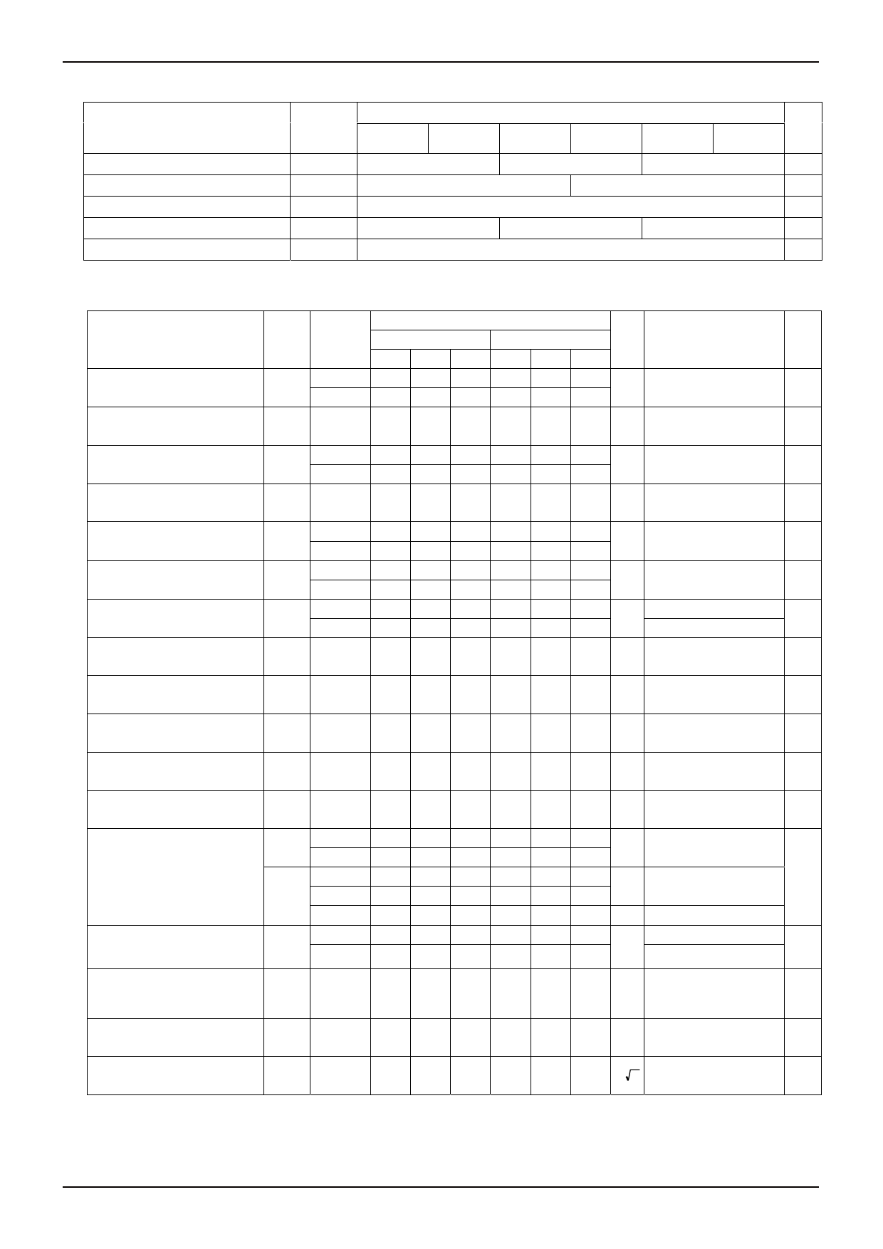
●Absolute Maximum Ratings (Ta=25[℃])
Parameter
Symbol
Supply Voltage
Operating Temperature Range
Storage Temperature Range
Input Common-mode Voltage
Maximum Junction Temperature
Vcc-GND
Topr
Tstg
VICM
Tjmax
LM358
family
LM324
family
+32
0 to +70
-0.3 to +32
Ratings
LM2904 LM2902
family
family
+26
LM2904V LM2902V Unit
family
family
+32
V
-40 to +125
℃
-65 to +150
℃
-0.3 to +26
-0.3 to +32
V
150
℃
●Electric Characteristics
○LM358,LM324 family (Unless otherwise specified, Vcc=+5[V])
Parameter
Limits
Symbol
Temperature
range
LM358 family
LM324 family
Unit
Conditions
Fig.
No
Min. Typ. Max. Min. Typ. Max.
Input Offset Voltage (*1)
25℃
-
3
7
-
3
7
VO=1.4[V]
VIO
mV VIC=VICR(min)
98
Full range -
-
9
-
-
9
Vcc=5[V] to 30[V]
Input Offset Voltage Drift
αVIO
-
-
7
-
-
-
- μV/℃
-
-
25℃
-
2
50
-
2
50
Input Offset Current (*1)
IIO
nA VO=1.4[V]
98
Full range -
-
150
-
-
150
Input Offset Current Drift
αIIO
-
-
10
-
-
-
- pA/℃
-
-
25℃
-
20
250
-
20 250
Input Bias Current (*1)
IIB
nA VO=1.4[V]
98
Full range -
-
500
-
-
500
25℃
0
- Vcc-1.5 -
- Vcc-1.5
Input Common-modeVoltage Range VICR
V Vcc=5[V] to 30[V]
98
Full range 0
- Vcc-2.0 -
- Vcc-2.0
High Level Output Voltage
25℃
Vcc-1.5 -
- Vcc-1.5 -
-
RL≧2[kΩ]
VOH
V
99
Full range 27
28
-
27
28
-
Vcc=30[V],RL≧10[kΩ]
Low Level Output Voltage
VOL Full range -
5
20
-
5
20 mV RL≦10[kΩ]
98
Large Signal Voltage Gain
AVD
25℃
25
100
-
Vcc=15[V]
25
100
- V/mV VO=1[V] to 11[V]
98
RL≧2[kΩ]
Common-mode Rejection Ratio
CMRR
25℃
65
80
-
65
80
-
dB
Vcc=5[V] to 30[V],
VIC=VICR(min)
98
Supply-Voltage rejection ratio
KSVR
25℃
65
100
-
65
100
-
dB Vcc=5[V] to 30[V]
98
Cross-talk Attenuation
VO1/VO2 25℃
-
120
-
-
120
-
dB f=1[kHz] to 20[kHz]
101
25℃
20
Source
Full range 10
30
-
-
-
20
10
30
-
-
-
mA
Vcc=15[V],VO=0[V]
VID=1[V]
Output Current (*2)
25℃
10
Sink Full range 2
20
-
-
-
10
2
20
-
-
-
mA
Vcc=15[V],VO=0[V]
VID=-1[V]
99
25℃
12
30
-
12
30
- μA VO=200[mV],VID=-1[V]
Supply Current (All Amps)
Full range -
0.7 1.2
-
0.7 1.2
VO=2.5[V],No Load
ICC
Full range -
1
2
-
1.4
3
mA Vcc=30[V],VO=0.5[V]
No Load
99
RL=1[MΩ],CL=30[pF]
Slew Rate at Unity-Gain
SR
25℃
-
0.3
-
-
0.5
-
V/μs
VI=±10[V]
Vcc=15[V],GND=-15[V]
99
(reference to Fig100)
Unity Gain Bandwidth
RL=1[MΩ],CL=20[pF]
B1
25℃
-
0.7
-
-
1.2
- MHz Vcc=15[V],GND=-15[V]
99
(reference to Fig99)
Equivalent Input Noise Voltage
Vcc=15[V],GND=-15[V]
Vn
25℃
-
40
-
-
35
- nV/ Hz RS=100[Ω],VI=0[V]
99
f=1[kHz](reference to Fig99)
(*1) Absolute value
(*2) Under high temperature, consider the power dissipation of IC when selecting the output current.
When the output terminal is continuously shorted, the output current reduces the temperature inside the IC by flushing.
www.rohm.com
© 2011 ROHM Co., Ltd. All rights reserved.
2/17
2011.06 - Rev.B
Share Link: 