BC489AG(2007) View Datasheet(PDF) - ON Semiconductor
Part Name
Description
Manufacturer
BC489AG Datasheet PDF : 6 Pages
| |||
BC489, BC489A
ELECTRICAL CHARACTERISTICS (TA = 25°C unless otherwise noted)
Characteristic
Symbol
Min
OFF CHARACTERISTICS
Collector −Emitter Breakdown Voltage (Note 1)
(IC = 10 mAdc, IB = 0)
V(BR)CEO
80
Collector −Base Breakdown Voltage
(IC = 100 mAdc, IE = 0)
V(BR)CBO
80
Emitter −Base Breakdown Voltage
(IE = 10 mAdc, IC = 0)
V(BR)EBO
5.0
Collector Cutoff Current
(VCB = 60 V, IE = 0)
ICBO
−
ON CHARACTERISTICS
DC Current Gain
(IC = 10 mAdc, VCE = 2.0 Vdc)
(IC = 100 mAdc, VCE = 2.0 Vdc)
hFE
40
BC489
60
BC489A
100
(IC = 1.0 Adc, VCE = 5.0 Vdc)
Collector −Emitter Saturation Voltage
(IC = 500 mAdc, IB = 50 mAdc)
(IC = 1.0 Adc, IB = 100 mAdc)
Collector −Emitter Saturation Voltage
(IC = 500 mAdc, IB = 50 mAdc)
(IC = 1.0 Adc, IB = 100 mAdc) (Note 1)
DYNAMIC CHARACTERISTICS
Current−Gain − Bandwidth Product
(IC = 50 mAdc, VCE = 2.0 Vdc, f = 100 MHz)
Output Capacitance
(VCB = 10 Vdc, IE = 0, f = 1.0 MHz)
Input Capacitance
(VEB = 0.5 Vdc, IC = 0, f = 1.0 MHz)
1. Pulse Test: Pulse Width = 300 ms, Duty Cycle 2.0%.
15
VCE(sat)
−
−
VBE(sat)
−
−
fT
−
Cob
−
Cib
−
Typ
−
−
−
−
−
−
160
−
0.2
0.3
0.85
0.9
200
7.0
50
Max
Unit
Vdc
−
Vdc
−
−
Vdc
nAdc
100
−
−
400
250
−
Vdc
0.5
−
Vdc
1.2
−
−
MHz
−
pF
−
pF
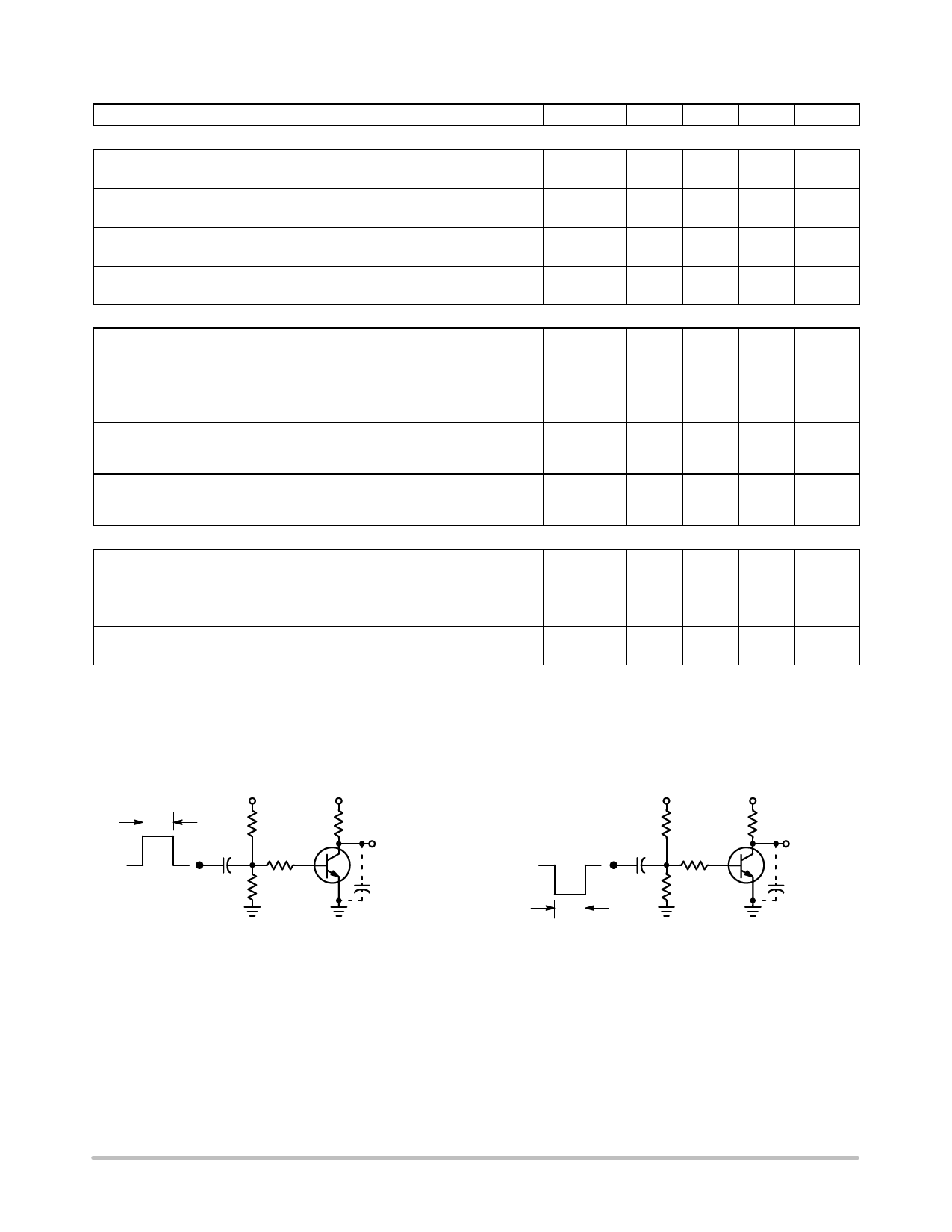
TURN−ON TIME
5.0 ms
−1.0 V
+10 V
0
tr = 3.0 ns
Vin
5.0 mF
100
RB
100
VCC
+40 V
RL
OUTPUT
*CS < 6.0 pF
TURN−OFF TIME
+VBB
100
Vin
RB
VCC
+40 V
RL
OUTPUT
5.0 mF 100
*CS < 6.0 pF
5.0 ms
tr = 3.0 ns
*Total Shunt Capacitance of Test Jig and Connectors For PNP Test Circuits, Reverse All Voltage Polarities
Figure 1. Switching Time Test Circuits
http://onsemi.com
2
Share Link: 