MJ14003 View Datasheet(PDF) - Motorola => Freescale
Part Name
Description
Manufacturer
MJ14003 Datasheet PDF : 6 Pages
| |||
ÎÎÎÎÎÎÎÎÎÎÎÎÎÎÎÎÎÎÎÎÎÎÎÎÎÎÎÎÎÎÎÎÎÎÎÎÎÎÎÎÎÎÎÎÎÎÎÎÎÎÎÎÎÎÎÎÎÎÎÎÎÎÎÎÎÎÎÎ MJ14002 MJ14001 MJ14003
ÎÎÎÎÎÎÎÎÎÎÎÎÎÎÎÎÎÎÎÎÎÎÎÎÎÎÎÎÎÎÎÎÎÎ ELECTRICAL CHARACTERISTICS (TC = 25_C unless otherwise noted)
ÎÎÎÎÎÎÎÎÎÎÎÎÎÎÎÎÎÎÎÎÎÎÎÎÎÎÎÎÎÎÎÎÎÎ Characteristic
Symbol
Min
ÎÎÎÎÎÎÎÎÎÎÎÎÎÎÎÎÎÎÎÎÎÎÎÎÎÎÎÎÎÎÎÎÎÎ OFF CHARACTERISTICS
ÎÎÎÎÎÎÎÎÎÎÎÎÎÎÎÎÎÎÎÎÎÎÎÎÎÎÎÎÎÎÎÎÎÎ Collector–Emitter Sustaining Voltage (1)
ÎÎÎÎÎÎÎÎÎÎÎÎÎÎÎÎÎÎÎÎÎÎÎÎÎÎÎÎÎÎÎÎÎÎ (IC = 200 mAdc, IB = 0)
MJ14001
VCEO(sus)
60
MJ14002, MJ14003
80
ÎÎÎÎÎÎÎÎÎÎÎÎÎÎÎÎÎÎÎÎÎÎÎÎÎÎÎÎÎÎÎÎÎÎ Collector Cutoff Current
ÎÎÎÎÎÎÎÎÎÎÎÎÎÎÎÎÎÎÎÎÎÎÎÎÎÎÎÎÎÎÎÎÎÎ (VCE = 30 Vdc, IB = 0)
ÎÎÎÎÎÎÎÎÎÎÎÎÎÎÎÎÎÎÎÎÎÎÎÎÎÎÎÎÎÎÎÎÎÎ (VCE = 40 Vdc, IB = 0)
ÎÎÎÎÎÎÎÎÎÎÎÎÎÎÎÎÎÎÎÎÎÎÎÎÎÎÎÎÎÎÎÎÎÎ Collector Cutoff Current
(VCE = 60 Vdc, VBE(off) = 1.5 V)
ÎÎÎÎÎÎÎÎÎÎÎÎÎÎÎÎÎÎÎÎÎÎÎÎÎÎÎÎÎÎÎÎÎÎ (VCE = 80 Vdc, VBE(off) = 1.5 V)
ÎÎÎÎÎÎÎÎÎÎÎÎÎÎÎÎÎÎÎÎÎÎÎÎÎÎÎÎÎÎÎÎÎÎ Collector Cutoff Current
ÎÎÎÎÎÎÎÎÎÎÎÎÎÎÎÎÎÎÎÎÎÎÎÎÎÎÎÎÎÎÎÎÎÎ (VCB = 60 Vdc, IE = 0)
(VCB = 80 Vdc, IE = 0)
ÎÎÎÎÎÎÎÎÎÎÎÎÎÎÎÎÎÎÎÎÎÎÎÎÎÎÎÎÎÎÎÎÎÎ Emitter Cutoff Current
ÎÎÎÎÎÎÎÎÎÎÎÎÎÎÎÎÎÎÎÎÎÎÎÎÎÎÎÎÎÎÎÎÎÎ (VBE = 5 Vdc, IC = 0)
MJ14001
ICEO
—
MJ14402, MJ14003
—
MJ14001
ICEX
—
MJ14002, MJ14003
—
MJ14001
ICBO
—
MJ14002, MJ14003
—
IEBO
—
ÎÎÎÎÎÎÎÎÎÎÎÎÎÎÎÎÎÎÎÎÎÎÎÎÎÎÎÎÎÎÎÎÎÎ ON CHARACTERISTICS
ÎÎÎÎÎÎÎÎÎÎÎÎÎÎÎÎÎÎÎÎÎÎÎÎÎÎÎÎÎÎÎÎÎÎ DC Current Gain (1)
ÎÎÎÎÎÎÎÎÎÎÎÎÎÎÎÎÎÎÎÎÎÎÎÎÎÎÎÎÎÎÎÎÎÎ (IC = 25 Adc, VCE = 3.0 V)
(IC = 50 Adc, VCE = 3.0 V)
ÎÎÎÎÎÎÎÎÎÎÎÎÎÎÎÎÎÎÎÎÎÎÎÎÎÎÎÎÎÎÎÎÎÎ (IC = 60 Adc, VCE = 3.0 V)
ÎÎÎÎÎÎÎÎÎÎÎÎÎÎÎÎÎÎÎÎÎÎÎÎÎÎÎÎÎÎÎÎÎÎ Collector–Emitter Saturation Voltage (1)
ÎÎÎÎÎÎÎÎÎÎÎÎÎÎÎÎÎÎÎÎÎÎÎÎÎÎÎÎÎÎÎÎÎÎ (IC = 25 Adc, IB = 2.5 Adc)
(IC = 50 Adc, IB = 5.0 Adc)
ÎÎÎÎÎÎÎÎÎÎÎÎÎÎÎÎÎÎÎÎÎÎÎÎÎÎÎÎÎÎÎÎÎÎ (IC = 60 Adc, IB = 12 Adc)
ÎÎÎÎÎÎÎÎÎÎÎÎÎÎÎÎÎÎÎÎÎÎÎÎÎÎÎÎÎÎÎÎÎÎ Base–Emitter Saturation Voltage (1)
(IC = 25 Adc, IB = 2.5 Adc)
ÎÎÎÎÎÎÎÎÎÎÎÎÎÎÎÎÎÎÎÎÎÎÎÎÎÎÎÎÎÎÎÎÎÎ (IC = 50 Adc, IB = 5.0 Adc)
ÎÎÎÎÎÎÎÎÎÎÎÎÎÎÎÎÎÎÎÎÎÎÎÎÎÎÎÎÎÎÎÎÎÎ (IC = 60 Adc, IB = 12 Adc)
ÎÎÎÎÎÎÎÎÎÎÎÎÎÎÎÎÎÎÎÎÎÎÎÎÎÎÎÎÎÎÎÎÎÎ DYNAMIC CHARACTERISTICS
ÎÎÎÎÎÎÎÎÎÎÎÎÎÎÎÎÎÎÎÎÎÎÎÎÎÎÎÎÎÎÎÎÎÎ Output Capacitance
(VCB = 10 Vdc, IE = 0, f = 0.1 MHz)
ÎÎÎÎÎÎÎÎÎÎÎÎÎÎÎÎÎÎÎÎÎÎÎÎÎÎÎÎÎÎÎÎÎÎ v (1) Pulse Test: Pulse Width = 300 µs, Duty Cycle 2%.
hFE
30
15
5
VCE(sat)
—
—
—
VBE(sat)
—
—
—
Cob
—
Max
Unit
Vdc
—
—
mA
1.0
1.0
mA
1.0
1.0
mA
1.0
1.0
1.0
mA
—
—
100
—
Vdc
1
2.5
3
Vdc
2
3
4
2000
pF
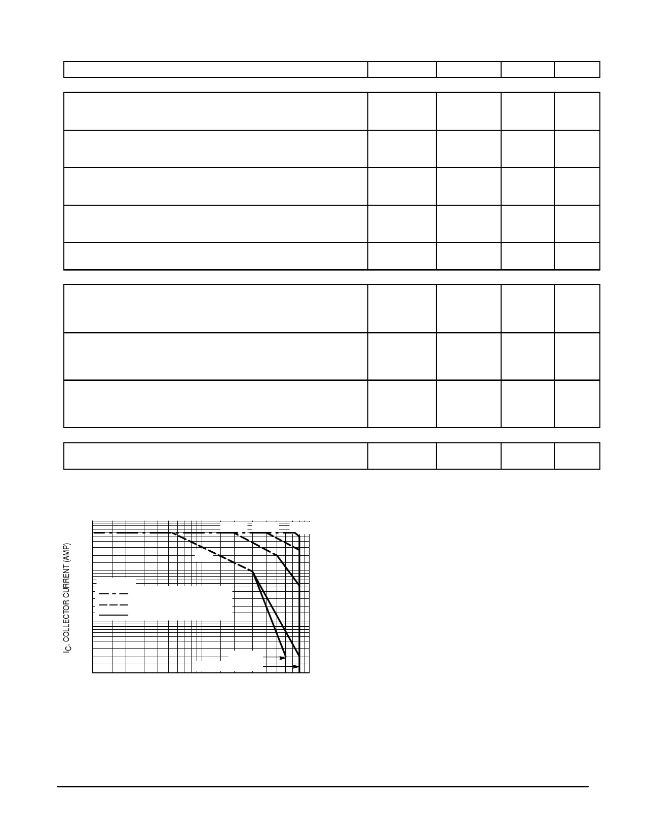
100
70
5.0 ms 1.0 ms 1.0 µs
50
30
20
dc
10
7.0
5.0
TC = 25°C
3.0
2.0
WIRE BOND LIMIT
THERMAL LIMIT
1.0
SECOND BREAKDOWN LIMIT
0.7
0.5
0.3
0.2
0.1
1.0
2.0 3.0
MJ14001
MJ14002, MJ14003
5.0 7.0 10
20 30 50 70 100
VCE, COLLECTOR–EMITTER VOLTAGE (VOLTS)
Figure 2. Maximum Rated Forward Biased
Safe Operating Area
There are two limitations on the power handling ability of a
transistor: average junction temperature and second break-
down. Safe operating area curves indicate IC – VCE limits of
the transistor that must be observed for reliable operation:
i.e., the transistor must not be subjected to greater dissipa-
tion than the curves indicate.
The data of Figure 2 is based on TJ(pk) = 200_C; TC is
variable depending on conditions. Second breakdown pulse
vlimits are valid for duty cycles to 10% provided TJ(pk)
200_C. TJ(pk) may be calculated from the data in Fig-
ure 13. At high case temperatures, thermal limitations will re-
duce the power that can be handled to values less than the
limitations imposed by second breakdown.
2
Motorola Bipolar Power Transistor Device Data
Share Link: 