FDP8880 View Datasheet(PDF) - Fairchild Semiconductor
Part Name
Description
Manufacturer
FDP8880 Datasheet PDF : 11 Pages
| |||
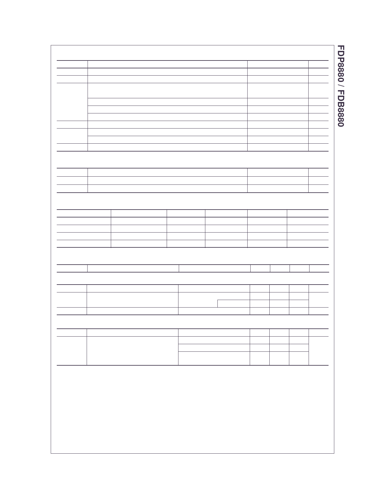
MOSFET Maximum Ratings TC = 25°C unless otherwise noted
Symbol
VDSS
VGS
ID
Parameter
Drain to Source Voltage
Gate to Source Voltage
Drain Current
Continuous (TC = 25oC, VGS = 10V)
Continuous (TC = 25oC, VGS = 4.5V)
Continuous (Tamb = 25oC, VGS = 10V, with RθJA = 43oC/W)
Pulsed
EAS
Single Pulse Avalanche Energy (Note 1)
Power dissipation
PD
Derate above 25oC
TJ, TSTG Operating and Storage Temperature
Ratings
30
±20
54
48
11
Figure 4
31
55
0.37
-55 to 175
Units
V
V
A
A
A
A
mJ
W
W/oC
oC
Thermal Characteristics
RθJC
RθJA
RθJA
Thermal Resistance Junction to Case TO-220,TO-263
Thermal Resistance Junction to Ambient TO-220,TO-262 ( Note 2)
Thermal Resistance Junction to Ambient TO-263, 1in2 copper pad area
2.73
62
43
oC/W
oC/W
oC/W
Package Marking and Ordering Information
Device Marking
FDP8880
FDB8880
FDP8880
FDB8880
Device
FDP8880
FDB8880
FDP8880_NL (Note 3)
FDB8880_NL (Note 3)
Package
TO-220AB
TO-263AB
TO-220AB
TO-263AB
Reel Size
Tube
330mm
Tube
330mm
Tape Width
N/A
24mm
N/A
24mm
Quantity
50 units
800 units
50 units
800 units
Electrical Characteristics TC = 25°C unless otherwise noted
Symbol
Parameter
Test Conditions
Off Characteristics
BVDSS
Drain to Source Breakdown Voltage
IDSS
Zero Gate Voltage Drain Current
IGSS
Gate to Source Leakage Current
ID = 250µA, VGS = 0V
VDS = 24V
VGS = 0V
TC = 150oC
VGS = ±20V
On Characteristics
VGS(TH)
Gate to Source Threshold Voltage
rDS(ON)
Drain to Source On Resistance
VGS = VDS, ID = 250µA
ID = 40A, VGS = 10V
ID = 40A, VGS = 4.5V
ID = 40A, VGS = 10V,
TJ = 175oC
Min Typ Max Units
30
-
-
V
-
-
1
µA
-
-
250
-
-
±100 nA
1.2
-
2.5
V
- 0.0095 0.0116
-
0.012 0.0145 Ω
- 0.015 0.019
©2005 Fairchild Semiconductor Corporation
2
FDP8880 / FDB8880 Rev. A
www.fairchildsemicom
Share Link: 