HV823(2001) View Datasheet(PDF) - Supertex Inc
Part Name
Description
Manufacturer
HV823 Datasheet PDF : 8 Pages
| |||
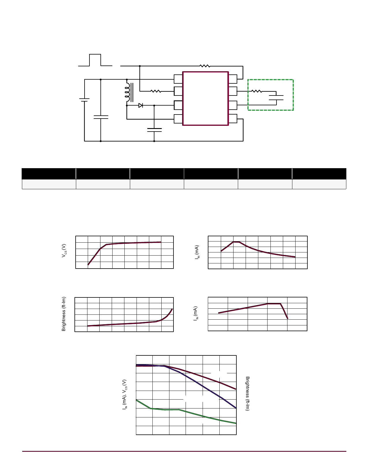
Block Diagram
VDD
RSW-osc
Enable *
GND
Switch
Osc
+
Disable C_
Vref
REL-osc
* Enable is available in die form only.
Q
Q
Output
Osc
Q
Q
HV823
Lx
Cs
VA
VB
Figure 1: Test Circuit, VIN = 3.0V (Low input current with moderate output brightness).
ON = VDD
OFF = 0V
2MΩ
VDD = VIN = 3.0V
560µH1
750KΩ
1N4148
0.1µF2
0.1µF
100V
1 VDD
REL-osc
8
2 RSW-osc
VA
7
3 Cs
VB
6
4 Lx
GND
5
HV823
2.0KΩ
10nF
Equivalent to 3 square inch lamp.
Typical Performance
Lamp Size VIN
3.0 in2
3.0v
IIN
VCS
fEL
Brightness
25mA 65v 385Hz 6.5ft-lm
Notes:
1. Murata part # LQH4N561K04 (DC resistance < 14.5Ω)
2. Larger values may be required depending upon supply impedance.
For additional information, see Application Notes AN-H33 and AN-H34.
3
Share Link: 