LD7577JAGR View Datasheet(PDF) - Unspecified
Part Name
Description
Manufacturer
LD7577JAGR Datasheet PDF : 20 Pages
| |||
LD7577JA
auxiliary winding of the transformer. Therefore, the
power losses on the startup circuit beyond the startup
period can be eliminated and the power saving can be
easily achieved. In general application, a 39KΩ resistor is
still recommended to be placed in high voltage path to
limit the current if there is a negative voltage applying in
any case.
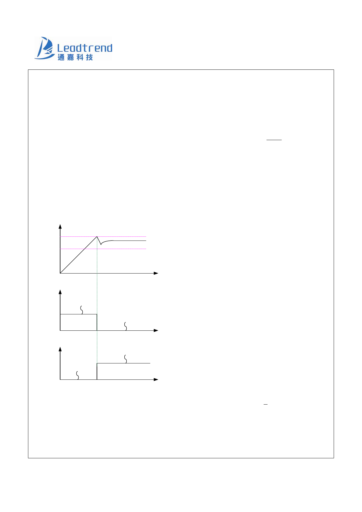
An UVLO comparator is included to detect the voltage on
the VCC pin to ensure the supply voltage is high enough to
power on the LD7577JA PWM controller and in addition to
drive the power MOSFET. As shown in Fig. 15, a
Hysteresis is provided to prevent the shutdown caused by
the voltage dip during startup. The turn-on and turn-off
threshold levels are set at 16V and 10.0V, respectively.
Vcc
UVLO(on)
UVLO(off)
t
HV Current
1mA
Vcc current
Startup Current
~ 0mA (off)
t
Operating Current
(Supply from Auxiliary Winding)
Fig. 15
Current Sensing, Leading-edge Blanking
and the Negative Spike on CS Pin
The typical current mode PWM controller feeds back both
current signal and voltage signal to close the control loop
and to achieve voltage regulation. LD7577JA detects the
primary MOSFET current from the CS pin, which is
applied not only for the peak current mode control but also
for the pulse-by-pulse current limit. The maximum voltage
threshold of the current sensing pin is set as 0.85V. Thus
the MOSFET peak current can be calculated as:
IPEAK(MAX)
=
0.85V
RS
A 250nS leading-edge blanking (LEB) time is incorporated
in the input of CS pin to prevent the false-trigger caused
by any current spike. For low power applications, if the
total pulse width of each turn-on spike is less than 250nS
and the negative spike on the CS pin is not as low as
-0.3V, the R-C filter (as shown in Fig.16) can be
eliminated. Nevertheless, it is strongly recommended to
remain a small R-C filter (as shown in Fig. 17) for higher
power applications to avoid the CS pin being damaged by
negative turn-on spikes.
Output Stage and Maximum Duty-Cycle
An output stage of a CMOS buffer, with typical 500mA
driving capability, is incorporated to drive a power
MOSFET directly. And the maximum duty-cycle of the
LD7577JA is limited to 75% in order to avoid the
transformer flux saturation.
Voltage Feedback Loop
The voltage feedback signal is issued from the TL431 in
the secondary side through the photo-coupler to COMP
pin of the LD7577JA. The input stage of the LD7577JA,
like the UC384X, is incorporated with 2 diodes voltage
offset circuit and a voltage divider with 1/3 ratio.
Therefore,
V+ (PWM COMPARATOR
)
=
1
3
× (VCOMP
−
2VF )
A pull-high resistor is embedded internally, eliminating
external corresponding components on a board.
Leadtrend Technology Corporation
LD7577JA-DS-00b August 2010
10
www.leadtrend.com.tw
Share Link: 