BSS92 View Datasheet(PDF) - Philips Electronics
Part Name
Description
Manufacturer
BSS92 Datasheet PDF : 8 Pages
| |||
Philips Semiconductors
P-channel enhancement mode
vertical D-MOS transistor
Product specification
BSS92
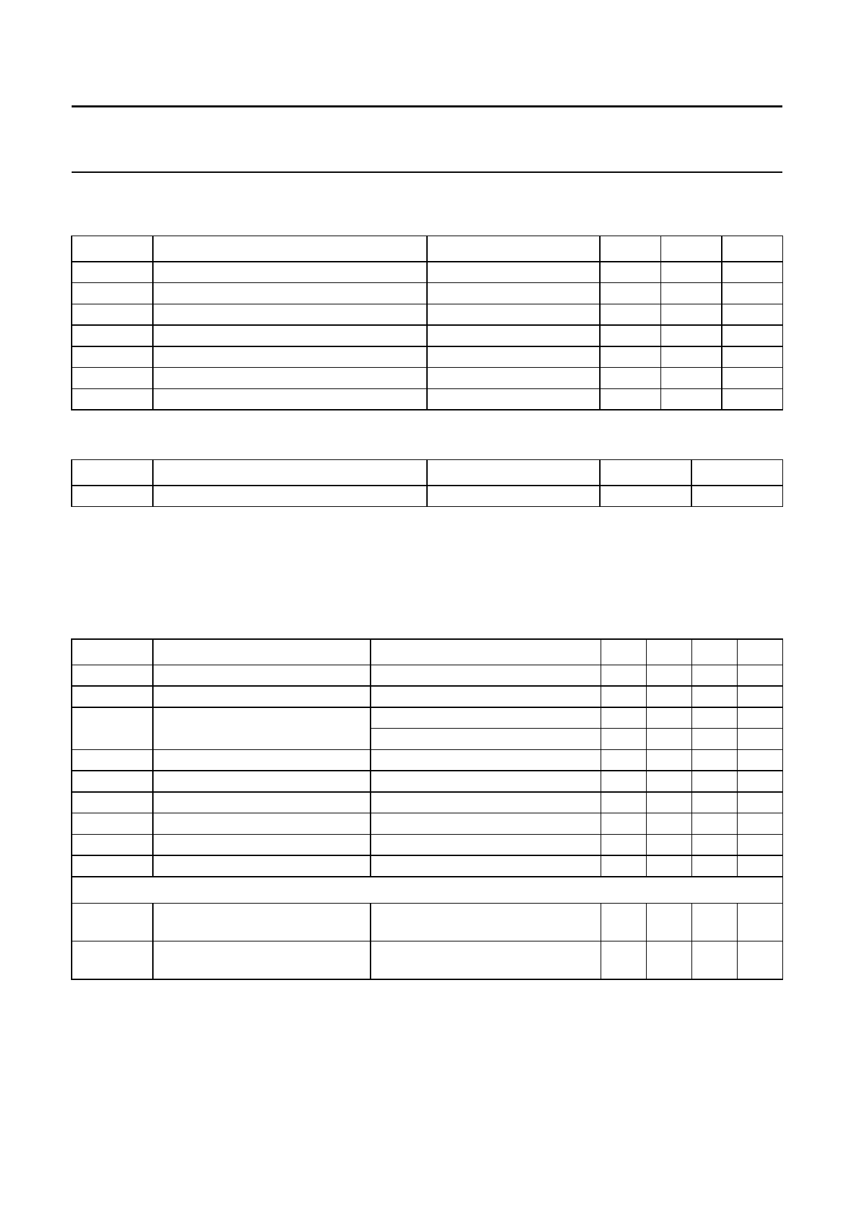
LIMITING VALUES
In accordance with the Absolute Maximum Rating System (IEC 134).
SYMBOL
PARAMETER
CONDITIONS
VDS
VGSO
ID
IDM
Ptot
Tstg
Tj
drain-source voltage (DC)
gate-source voltage (DC)
drain current (DC)
peak drain current
total power dissipation
storage temperature
operating junction temperature
open drain
Tamb ≤ 25 °C; note 1
MIN.
−
−
−
−
−
−55
−
MAX.
−240
±20
−150
−600
1
+150
150
UNIT
V
V
mA
mA
W
°C
°C
THERMAL CHARACTERISTICS
SYMBOL
PARAMETER
CONDITIONS
VALUE
UNIT
Rth j-a
thermal resistance from junction to ambient note 1
125
K/W
Note to the Limiting values and Thermal characteristics
1. Device mounted on a printed-circuit board, maximum lead length 4 mm; mounting pad for drain lead minimum
10 mm × 10 mm.
CHARACTERISTICS
Tj = 25 °C unless otherwise specified.
SYMBOL
PARAMETER
V(BR)DSS
VGSth
IDSS
drain-source breakdown voltage
gate-source threshold voltage
drain-source leakage current
IGSS
RDSon
yfs
Ciss
Coss
Crss
gate leakage current
drain-source on-state resistance
forward transfer admittance
input capacitance
output capacitance
reverse transfer capacitance
Switching times (see Figs 2 and 3)
ton
turn-on time
toff
turn-off time
CONDITIONS
VGS = 0; ID = −250 µA
VDS = VGS; ID = −1 mA
VGS = 0; VDS = −60 V
VGS = 0; VDS = −200 V
VDS = 0; VGS = ±20 V
VGS = −10 V; ID = −100 mA
VDS = −25 V; ID = −100 mA
VGS = 0; VDS = −25 V; f = 1 MHz
VGS = 0; VDS = −25 V; f = 1 MHz
VGS = 0; VDS = −25 V; f = 1 MHz
VGS = 0 to −10 V; VDD = −50 V;
ID = −250 mA
VGS = −10 to 0 V; VDD = −50 V;
ID = −250 mA
MIN. TYP. MAX. UNIT
−240 −
−
V
−0.8 −
−2.8 V
−
−
−200 nA
−
−
−60 µA
−
−
±100 nA
−
10 20 Ω
60 200 −
mS
−
65 −
pF
−
20 −
pF
−
6
−
pF
−
5
−
ns
−
20 −
ns
1997 Jun 19
3
Share Link: 