MC1489A View Datasheet(PDF) - ON Semiconductor
Part Name
Description
Manufacturer
MC1489A Datasheet PDF : 12 Pages
| |||
MC1489, MC1489A
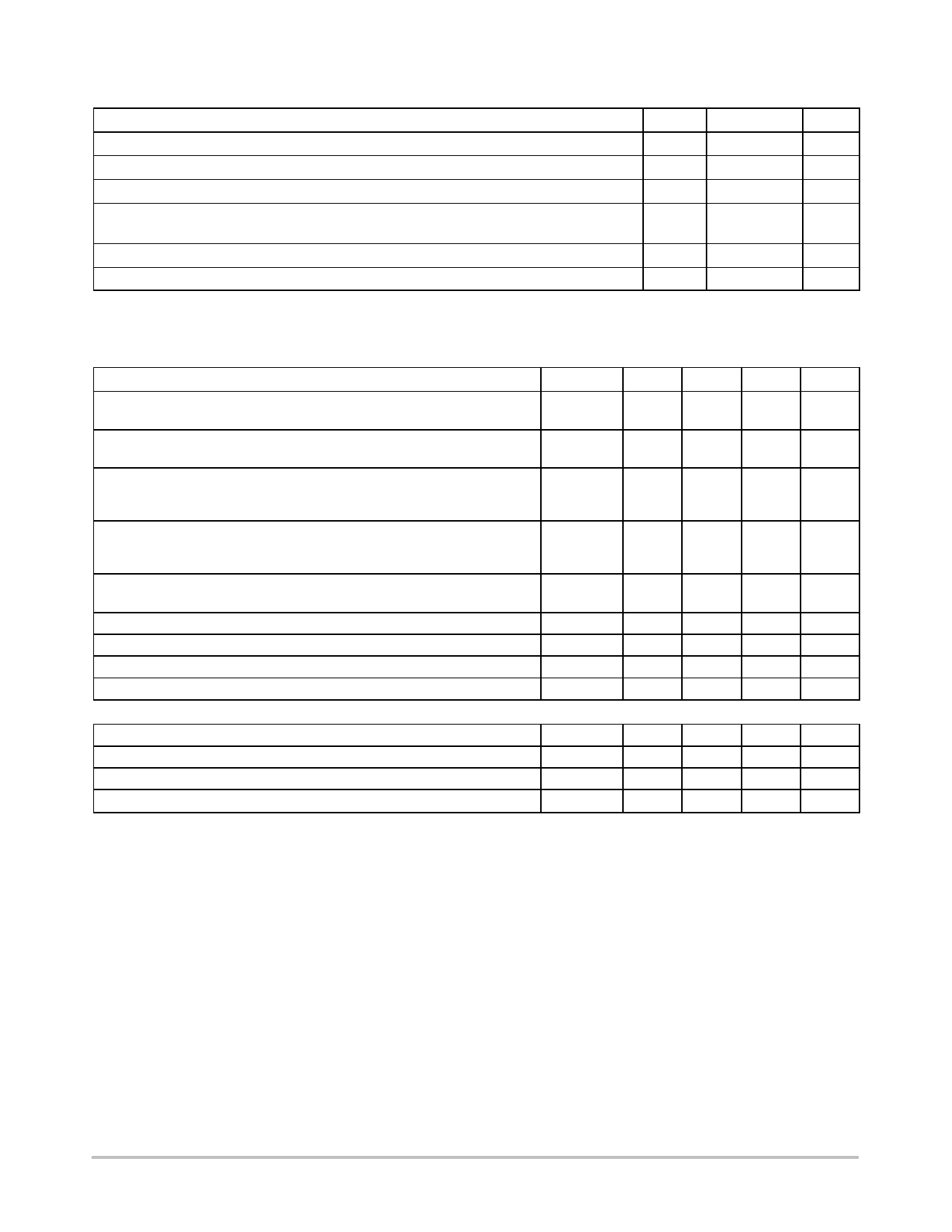
MAXIMUM RATINGS (TA = + 25°C, unless otherwise noted)
Rating
Symbol
Value
Unit
Power Supply Voltage
Input Voltage Range
Output Load Current
Power Dissipation (Package Limitation, SOIC−14 and Plastic Dual In−Line Package)
Derate above TA = + 25°C
VCC
VIR
IL
PD
1/qJA
10
± 30
20
1000
6.7
Vdc
Vdc
mA
mW
mW/°C
Operating Ambient Temperature Range
TA
0 to + 75
°C
Storage Temperature Range
Tstg
− 65 to + 175
°C
Stresses exceeding Maximum Ratings may damage the device. Maximum Ratings are stress ratings only. Functional operation above the
Recommended Operating Conditions is not implied. Extended exposure to stresses above the Recommended Operating Conditions may affect
device reliability.
ELECTRICAL CHARACTERISTICS (Response control pin is open.) (VCC = + 5.0 Vdc ± 10%, TA = 0 to + 75°C, unless otherwise noted)
Characteristics
Symbol
Min
Typ
Max
Unit
Positive Input Current
Negative Input Current
Input Turn−On Threshold Voltage
(TA = + 25°C, VOL p 0.45 V)
(VIH = + 25 Vdc)
(VIH = + 3.0 Vdc)
(VIH = − 25 Vdc)
(VIH = − 3.0 Vdc)
MC1489
MC1489A
IIH
3.6
−
8.3
mA
0.43
−
−
IIL
− 3.6
−
− 8.3
mA
− 0.43
−
−
VIH
Vdc
1.0
−
1.5
1.75
1.95
2.25
Input Turn−Off Threshold Voltage
(TA = + 25°C, VOH q 2.5 V, IL = − 0.5 mA)
MC1489
MC1489A
VIL
Vdc
0.75
−
1.25
0.75
0.8
1.25
Output Voltage High
(VIH = 0.75 V, IL = − 0.5 mA)
(Input Open Circuit, IL = − 0.5 mA)
VOH
2.5
4.0
5.0
Vdc
2.5
4.0
5.0
Output Voltage Low
Output Short−Circuit Current
(VIL = 3.0 V, IL = 10 mA)
Power Supply Current (All Gates “on,” Iout = 0 mA, VIH = + 5.0 Vdc)
VOL
−
0.2
0.45
Vdc
IOS
−
− 3.0 − 4.0
mA
ICC
−
16
26
mA
Power Consumption
(VIH = + 5.0 Vdc)
PC
SWITCHING CHARACTERISTICS (VCC = 5.0 Vdc ± 1%, TA = + 25°C, See Figure 3.)
Propagation Delay Time
(RL = 3.9 kW)
tPLH
Rise Time
(RL = 3.9 kW)
tTLH
Propagation Delay Time
(RL = 390 kW)
tPHL
Fall Time
(RL = 390 kW)
tTHL
−
80
130
mW
−
25
85
ns
−
120
175
ns
−
25
50
ns
−
10
20
ns
http://onsemi.com
3
Share Link: 