MC1489DR2 View Datasheet(PDF) - ON Semiconductor
Part Name
Description
Manufacturer
MC1489DR2 Datasheet PDF : 12 Pages
| |||
MC1489, MC1489A
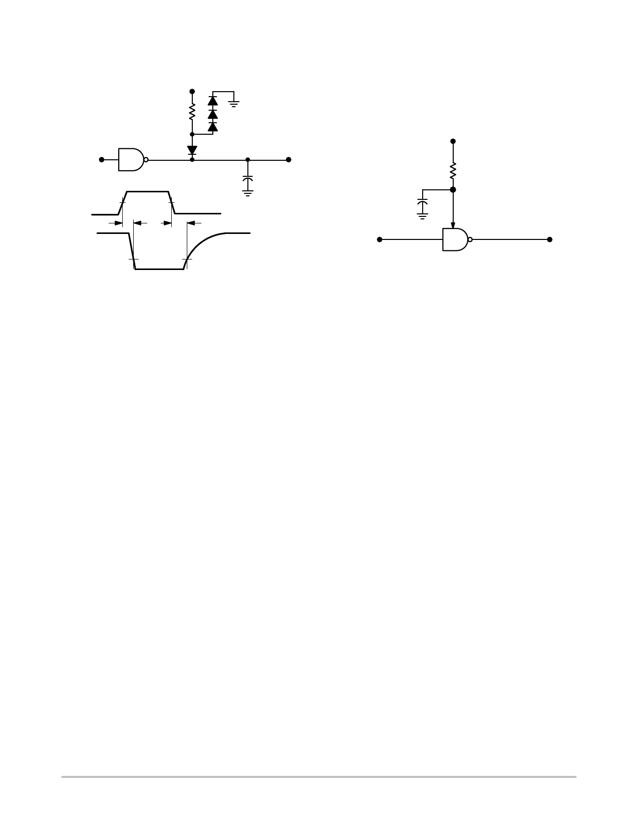
TEST CIRCUITS
5.0 Vdc
RL
All diodes
1N3064
or equivalent
Ein
3.0 V
50%
50%
Ein
tPLH
EO
tTHL 1.5 V
tTLH
1.5 V
Eo
CL
tTLH and tTHL
measured
10% - 90%
CL = 15 pF = total parasitic capacitance which includes
probe and wiring capacitances
Figure 3. Switching Response
VR
R
C
1/4
Response Node
MC1489A
Vin
VO
C, capacitor is for noise filtering.
R, resistor is for threshold shifting.
Figure 4. Response Control Node
http://onsemi.com
4
Share Link: 