RT9018A12PSP View Datasheet(PDF) - Richtek Technology
Part Name
Description
Manufacturer
RT9018A12PSP Datasheet PDF : 12 Pages
| |||
RT9018A/B
PD (MAX) = (125°C − 25°C) / (75°C/W) = 1.33W (SOP-8
Exposed Pad on the minimum layout)
Layout Considerations
The thermal resistance θJA of SOP-8 (Exposed Pad) is
determined by the package design and the PCB design.
However, the package design had been designed. If
possible, it’ s useful to increase thermal performance by
the PCB design. The thermal resistance θJA can be
decreased by adding a copper under the exposed pad of
SOP-8 (Exposed Pad) package.
As shown in Figure 3, the amount of copper area to which
the SOP-8 (Exposed Pad) is mounted affects thermal
performance. When mounted to the standard SOP-8
(Exposed Pad) pad (Figure 3.a), θJA is 75°C/W. Adding
copper area of pad under the SOP-8 (Exposed Pad) Figure
3.b) reduces the θJA to 64°C/W. Even further, increasing
the copper area of pad to 70mm2 (Figure 3.e) reduces the
θJA to 49° C/W.
Figure 3 (d). Copper Area = 50mm2, θJA = 51°C/W
Figure 3 (e). Copper Area = 70mm2, θJA = 49°C/W
Figure 3. Thermal Resistance vs. Different Cooper Area
Layout Design
Figure 3 (a). Minimum Footprint, θJA = 75°C/W
Figure 3 (b). Copper Area = 10mm2, θJA = 64°C/W
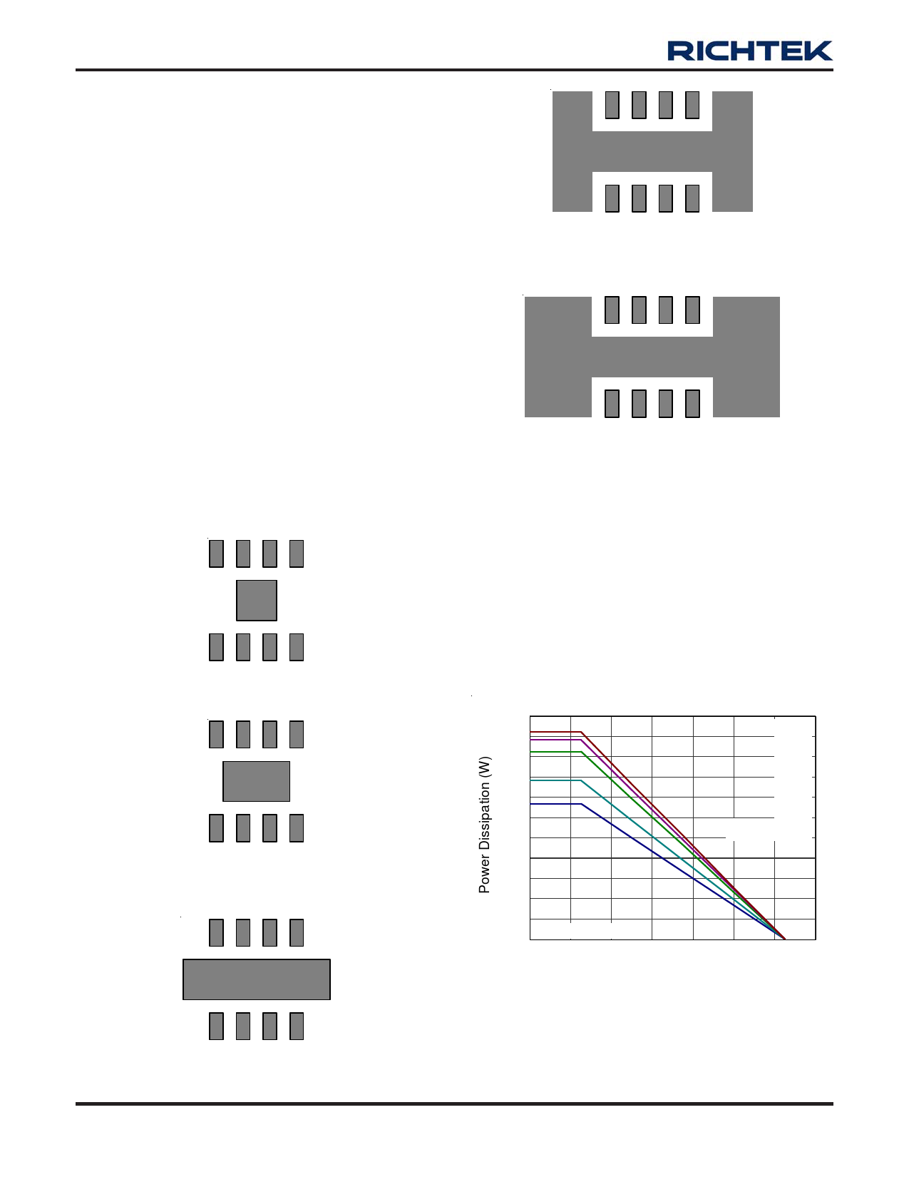
The maximum power dissipation depends on operating
ambient temperature for fixed TJ(MAX) and thermal
resistance θJA . For RT9018A/B packages, the Figure 4
of de-rating curves allows the designer to see the effect of
rising ambient temperature on the maximum power
allowed.
2.2
Copper Area
2
70mm2
1.8
50mm2
1.6
30mm2
1.4
1.2
10mm2
Minimum Layout
1
0.8
0.6
0.4
0.2
JEDEC 4-Layers PCB
0
0
20 40 60
80 100 120 140
Ambient Temperature (°C)
Figure 4. De-rating Curves
Figure 3 (c). Copper Area = 30mm2, θJA = 54°C/W
www.richtek.com
10
DS9018A/B-04 September 2007
Share Link: 