MUN2113T1G(2012) View Datasheet(PDF) - ON Semiconductor
Part Name
Description
Manufacturer
MUN2113T1G Datasheet PDF : 12 Pages
| |||
MUN2113, MMUN2113L, MUN5113, DTA144EE, DTA144EM3, NSBA144EF3
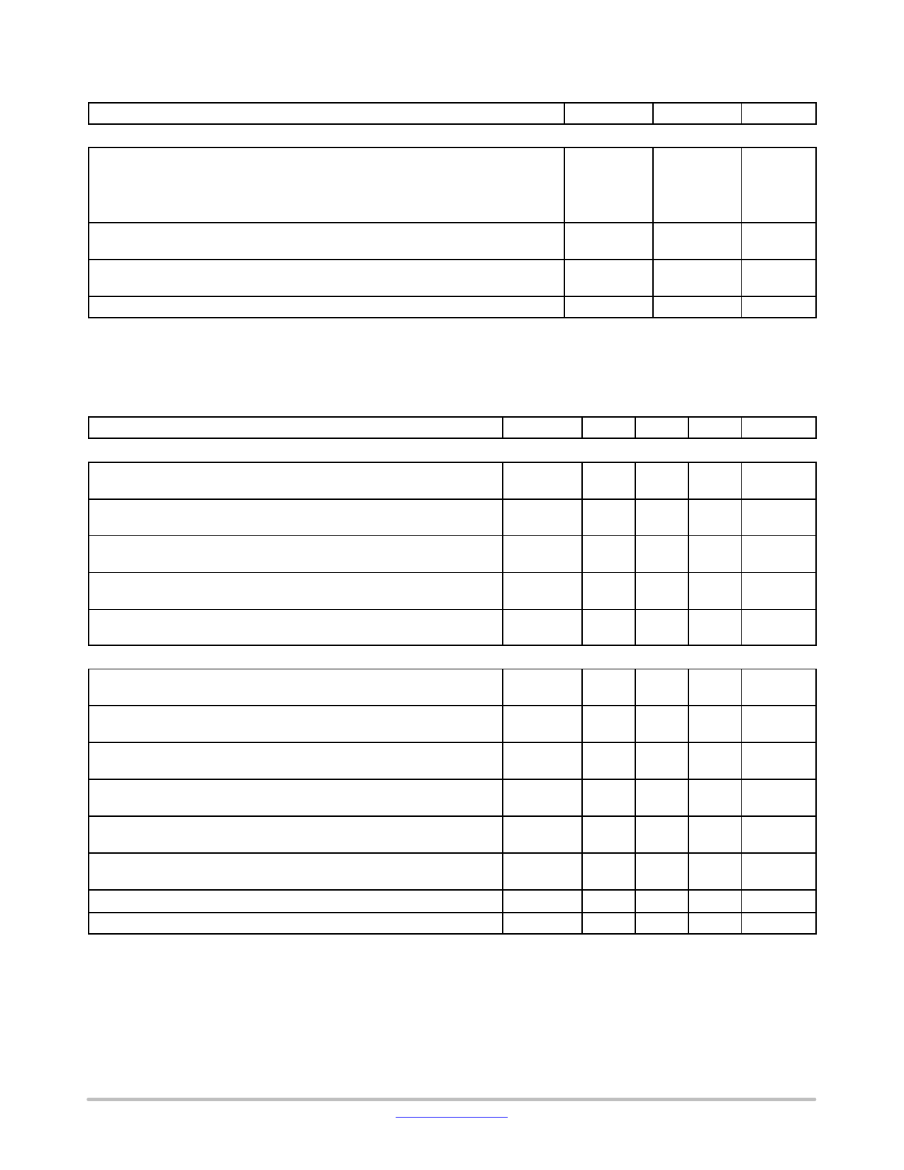
Table 2. THERMAL CHARACTERISTICS
Characteristic
THERMAL CHARACTERISTICS (SOT−1123) (NSBA144EF3)
Total Device Dissipation
TA = 25°C
Derate above 25°C
Thermal Resistance,
Junction to Ambient
Thermal Resistance, Junction to Lead
Junction and Storage Temperature Range
1. FR−4 @ Minimum Pad.
2. FR−4 @ 1.0 x 1.0 Inch Pad.
3. FR−4 @ 100 mm2, 1 oz. copper traces, still air.
4. FR−4 @ 500 mm2, 1 oz. copper traces, still air.
Symbol
Max
(Note 3)
(Note 4)
(Note 3)
(Note 4)
(Note 3)
(Note 4)
(Note 3)
PD
RqJA
RqJL
TJ, Tstg
254
297
2.0
2.4
493
421
193
−55 to +150
Table 3. ELECTRICAL CHARACTERISTICS (TA = 25°C, unless otherwise noted)
Characteristic
Symbol
Min
Typ
Max
OFF CHARACTERISTICS
Collector−Base Cutoff Current
(VCB = 50 V, IE = 0)
ICBO
−
−
100
Collector−Emitter Cutoff Current
(VCE = 50 V, IB = 0)
ICEO
−
−
500
Emitter−Base Cutoff Current
(VEB = 6.0 V, IC = 0)
IEBO
−
−
0.1
Collector−Base Breakdown Voltage
(IC = 10 mA, IE = 0)
V(BR)CBO
50
−
−
Collector−Emitter Breakdown Voltage (Note 5)
(IC = 2.0 mA, IB = 0)
V(BR)CEO
50
−
−
ON CHARACTERISTICS
DC Current Gain (Note 5)
(IC = 5.0 mA, VCE = 10 V)
hFE
80
140
−
Collector−Emitter Saturation Voltage (Note 5)
(IC = 10 mA, IB = 0.3 mA)
VCE(sat)
−
−
0.25
Input Voltage (off)
(VCE = 5.0 V, IC = 100 mA)
Vi(off)
−
1.2
−
Input Voltage (on)
(VCE = 0.2 V, IC = 3.0 mA)
Vi(on)
−
2.0
−
Output Voltage (on)
(VCC = 5.0 V, VB = 3.5 V, RL = 1.0 kW)
VOL
−
−
0.2
Output Voltage (off)
(VCC = 5.0 V, VB = 0.5 V, RL = 1.0 kW)
VOH
4.9
−
−
Input Resistor
R1
32.9
47
61.1
Resistor Ratio
5. Pulsed Condition: Pulse Width = 300 msec, Duty Cycle ≤ 2%.
R1/R2
0.8
1.0
1.2
Unit
mW
mW/°C
°C/W
°C/W
°C
Unit
nAdc
nAdc
mAdc
Vdc
Vdc
Vdc
Vdc
Vdc
Vdc
Vdc
kW
http://onsemi.com
4
Share Link: 