AD5301 View Datasheet(PDF) - Analog Devices
Part Name
Description
Manufacturer
AD5301 Datasheet PDF : 16 Pages
| |||
AD5301/AD5311/AD5321
The output voltage for any input code can be calculated as
VOUT = [(VDD × (D/2N) × (R1 + R2)/R1) – VDD × (R2/R1)]
where D is the decimal equivalent of the code loaded to the
DAC.
N is the DAC resolution.
With VDD = 5 V, R1 = R2 = 10 kΩ,
VOUT = (10 × D/2N) – 5 V
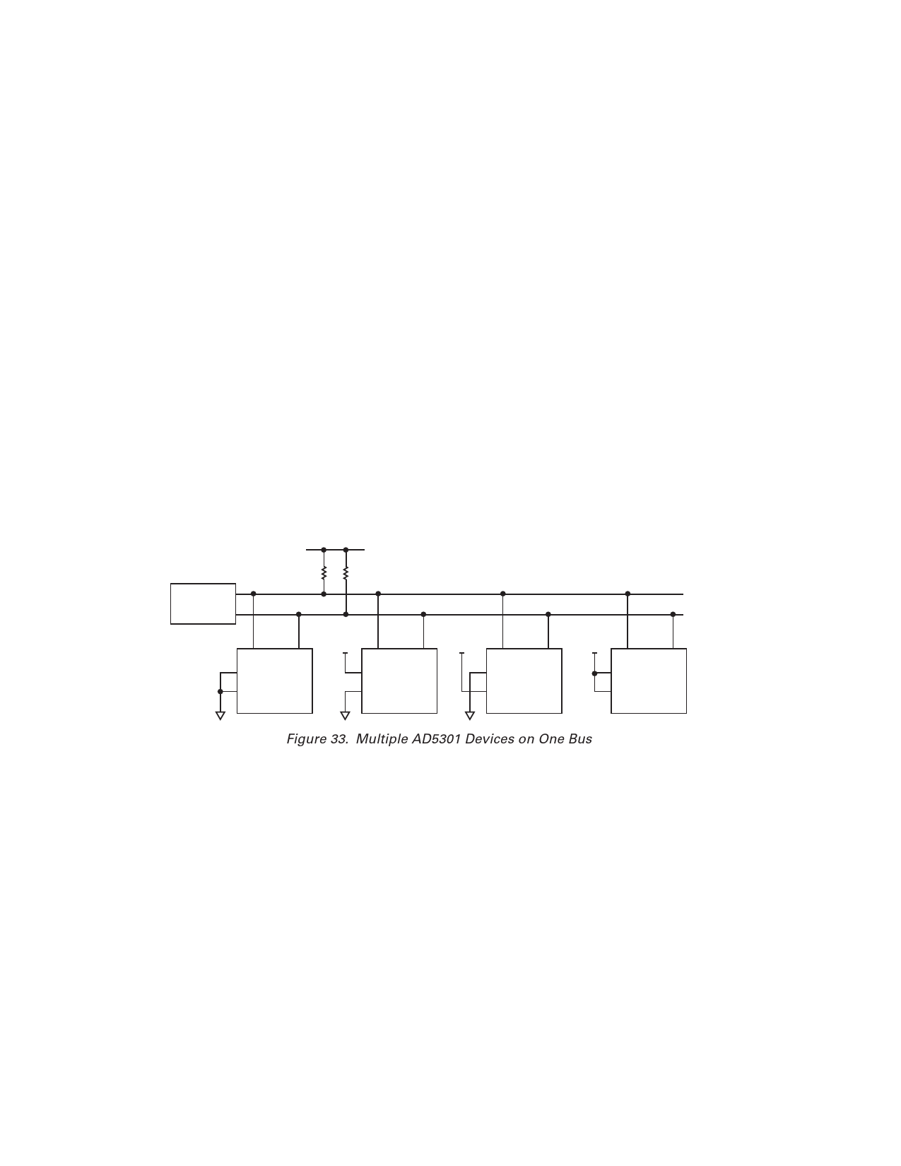
Multiple Devices on One Bus
Figure 33 shows four AD5301 devices on the same serial bus.
Each has a different slave address since the state of their A0 and
A1 pins is different. This allows each DAC to be written to or
read from independently. The master device output bus line
drivers are open-drain pull downs in a fully I2C-compatible
interface.
CMOS Driven SCL and SDA Lines
For single or multisupply systems where the minimum SCL
swing requirements allow it, a CMOS SCL driver may be used,
the SCL pull-up resistor can be removed, making the SCL bus
line fully CMOS compatible. This will reduce power consump-
tion in both the SCL driver and receiver devices. The SDA line
remains open-drain, I2C compatible.
Further changes, in the SDA line driver, may be made to make
the system more CMOS compatible and save more power. As
the SDA line is bidirectional, it cannot be made fully CMOS
compatible. A switched pull-up resistor can be combined with a
CMOS device with an open-circuit (three-state) input such that
the CMOS SDA driver is enabled during write cycles and I2C
mode is enabled during shared cycles, i.e., readback, acknowledge
bit cycles, start and stop conditions.
Power Supply Decoupling
In any circuit where accuracy is important, careful consideration
of the power supply and ground return layout helps to ensure
the rated performance. The AD5301/AD5311/AD5321 should
be decoupled to GND with a 10 µF in parallel with 0.1 µF
capacitor, located as close to the package as possible. The 10 µF
capacitor should be the tantalum bead type, while a ceramic
0.1 µF capacitor will provide a sufficient low impedance path
to ground at high frequencies. The power supply lines of the
AD5301/AD5311/AD5321 should use as large a trace as possible
to provide low impedance paths. A ground line routed between the
SDA and SCL lines will help reduce crosstalk between them (not
required on a multilayer board as there will be a ground plane layer
but separating the lines will help).
MASTER
5V
RP
RP
SDA
SCL
SDA
SCL
A1
VOUT
A0
AD5301
VDD
SDA
VDD
SCL
SDA
SCL
A1
VOUT
A0
AD5301
A1
VOUT
A0
AD5301
VDD
SDA
SCL
A1
VOUT
A0
AD5301
Figure 33. Multiple AD5301 Devices on One Bus
–14–
REV. A
Share Link: 