74LVC00ADB,112 View Datasheet(PDF) - NXP Semiconductors.
Part Name
Description
Manufacturer
74LVC00ADB,112 Datasheet PDF : 14 Pages
| |||
Nexperia
74LVC00A
Quad 2-input NAND gate
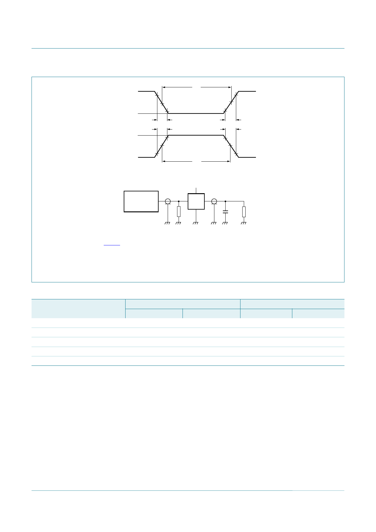
tW
VI 90 %
negative
pulse
VM
10 %
0V
tf
VI
positive
pulse
tr
90 %
VM
10 %
0V
tW
VM
tr
tf
VM
VCC
VI
PULSE
GENERATOR
VO
DUT
RT
CL
RL
001aaf615
Fig 7.
Test data is given in Table 8. Definitions for test circuit:
RL = Load resistance
CL = Load capacitance including jig and probe capacitance
RT = Termination resistance should be equal to output impedance Zo of the pulse generator
Load circuitry for measuring switching times
Table 8. Test data
Supply voltage
1.2 V
1.65 V to 1.95 V
2.3 V to 2.7 V
2.7 V
3.0 V to 3.6 V
Input
VI
VCC
VCC
VCC
2.7 V
2.7 V
tr, tf
≤ 2 ns
≤ 2 ns
≤ 2 ns
≤ 2.5 ns
≤ 2.5 ns
Load
CL
30 pF
30 pF
30 pF
50 pF
50 pF
RL
1 kΩ
1 kΩ
500 Ω
500 Ω
500 Ω
74LVC00A
Product data sheet
All information provided in this document is subject to legal disclaimers.
Rev. 7 — 25 April 2012
© Nexperia B.V. 2017. All rights reserved
6 of 14
Share Link: 