M62364FP View Datasheet(PDF) - Renesas Electronics
Part Name
Description
Manufacturer
M62364FP Datasheet PDF : 9 Pages
| |||
M62364FP/GP
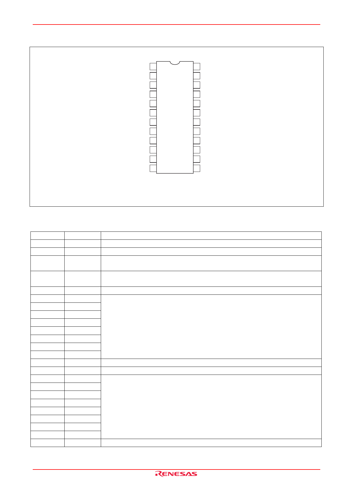
Pin Arrangement
M62364FP/GP
VIN1 1
VOUT1 2
VOUT2 3
VIN2 4
VDD 5
LD 6
CLK 7
DI 8
VIN3 9
VOUT3 10
VOUT4 11
VIN4 12
24 VIN8
23 VOUT8
22 VOUT7
21 VIN7
20 GND
19 RESET
18 VDAref
17 Do
16 VIN6
15 VOUT6
14 VOUT5
13 VIN5
(Top view)
Outline: PRSP0024GA-A (24P2Q-A)
PLSP0024JA-A (24P2E-A)
Pin Description
Pin No.
8
17
7
Pin Name
DI
DO
CLK
6
LD
19
RESET
2
VOUT1
3
VOUT2
10
VOUT3
11
VOUT4
14
VOUT5
15
VOUT6
22
VOUT7
23
VOUT8
5
VDD
20
GND
1
VIN1
4
VIN2
9
VIN3
12
VIN4
13
VIN5
16
VIN6
21
VIN7
24
VIN8
18
VDAref
Function
Serial data input
Serial data output
Shift clock input. Input data of DI are taken into the 12-bit shift register on a rising edge of
the clock.
A low state enables data loading to the 12-bit shift register.
During a rising edge of LD, the data will be loaded to the output register.
Reset 8-bit latches
D/A converter output with 8-bit resolution
Power supply
Ground
D/A converter input
D/A converter reference voltage input
REJ03D0875-0400 Rev.4.00 Oct 02, 2009
Page 2 of 8
Share Link: 