2SB1197-P-TP-HF View Datasheet(PDF) - Micro Commercial Components
Part Name
Description
Manufacturer
2SB1197-P-TP-HF Datasheet PDF : 2 Pages
| |||
MCC
TM
Micro Commercial Components
omponents
20736 Marilla Street Chatsworth
!"#
$%
!"#
2SB1197-P
2SB1197-Q
2SB1197-R
Features
• Lead Free Finish/RoHS Compliant ("P" Suffix designates
RoHS Compliant. See ordering information)
• Small Package
• Mounting:any position
• Epoxy meets UL 94 V-0 flammability rating
• Moisure Sensitivity Level 1
• Halogen free available upon request by adding suffix "-HF"
Maximum Ratings @ Ta = 25ć(unless otherwise noted)
Symbol
Parameter
Value
IC
Collector Current
-0.8
PD
Total Device Dissipation
0.2
TJ
Junction Temperature
150
TSTG
Storage Temperature Range
-55 to +150
Unit
A
W
к
к
Electrical Characteristics @ 25OC Unless Otherwise Specified
Symbol
Parameter
Min
OFF CHARACTERISTICS
V(BR)CEO
Collector-Emitter Breakdown Voltage
(IC=-1mAdc,IB=0)
-32
V(BR)CBO
Collector-Base Breakdown Voltage
(IC=-50uAdc,IE=0)
-40
V(BR)EBO
Collector-Base Breakdown Voltage
(IE=-50uAdc,IC=0)
-5.0
ICBO
Collector-Base Cutoff Current
(VCB=-20Vdc, IE=0)
IEBO
Emitter-Base Cutoff Current
(VEB=-4.0Vdc, IC=0)
ON CHARACTERISTICS
hFE
DC Current Gain
(IC=-100mAdc, VCE=-3.0Vdc)
82
VCE(sat)
Collector-Emitter Saturation Voltage
(IC=-500mAdc, IB=-50mAdc)
fT
Transition Frequency
(VCE=-5Vdc,IC=-50mAdc,f=100MHZ)
50
h CLASSIFICATION OF FE
Rank
P
Q
Range
82-180
120-270
Marking
AHP
AHQ
Max
Units
V
V
V
-0.5
µAdc
-0.5
uAdc
390
-0.5
Vdc
MHZ
R
180-390
AHR
PNP Silicon
Epitaxial Transistors
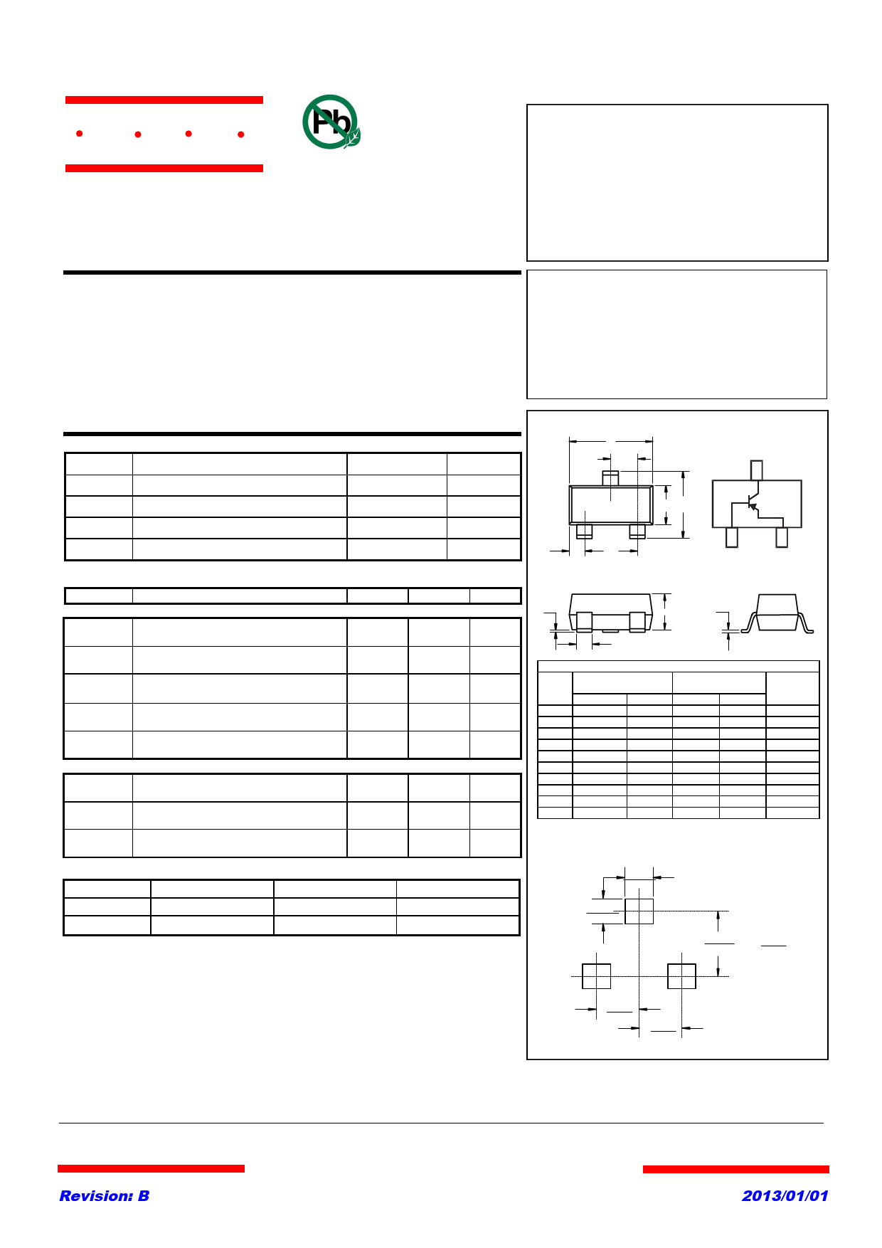
SOT-23
A
D
C
CB
F
E
B
E
G
H
J
K
DIMENSIONS
INCHES
DIM
MIN
MAX
A
.110
.120
B
.083
.104
C
.047
.055
D
.035
.041
E
.070
.081
F
.018
.024
G
.0005
.0039
H
.035
.044
J
.003
.007
K
.015
.020
MM
MIN
MAX
2.80
3.04
2.10
2.64
1.20
1.40
.89
1.03
1.78
2.05
.45
.60
.013
.100
.89
1.12
.085
.180
.37
.51
Suggested Solder
Pad Layout
NOTE
.031
.800
.035
.900
.079
2.000
inches
mm
.037
.950
.037
.950
Revision: B
w w w.mccsemi.com
1 of 2
2013/01/01
Share Link: 