BSP254A View Datasheet(PDF) - Philips Electronics
Part Name
Description
Manufacturer
BSP254A Datasheet PDF : 12 Pages
| |||
Philips Semiconductors
P-channel enhancement mode vertical
D-MOS transistor
LIMITING VALUES
In accordance with the Absolute Maximum System (IEC 134)
SYMBOL
−VDS
V GSO
−ID
−IDM
Ptot
Tstg
Tj
PARAMETER
drain-source voltage
gate-source voltage
drain current
drain current
total power dissipation
storage temperature range
junction temperature
CONDITIONS
open drain
DC
peak value
Tamb = 25 °C (note 1)
THERMAL RESISTANCE
SYMBOL
PARAMETER
Rth j-a
from junction to ambient (note 1)
Note
1. Transistor mounted on printed circuit board, maximum lead length 4 mm,
mounting pad for drain lead minimum 10 mm x 10 mm.
Product specification
BSP254; BSP254A
MIN.
−
−
−
−
−
−65
−
MAX.
250
20
0.2
0.6
1
+150
150
UNIT
V
V
A
A
W
°C
°C
MAX. UNIT
125
K/W
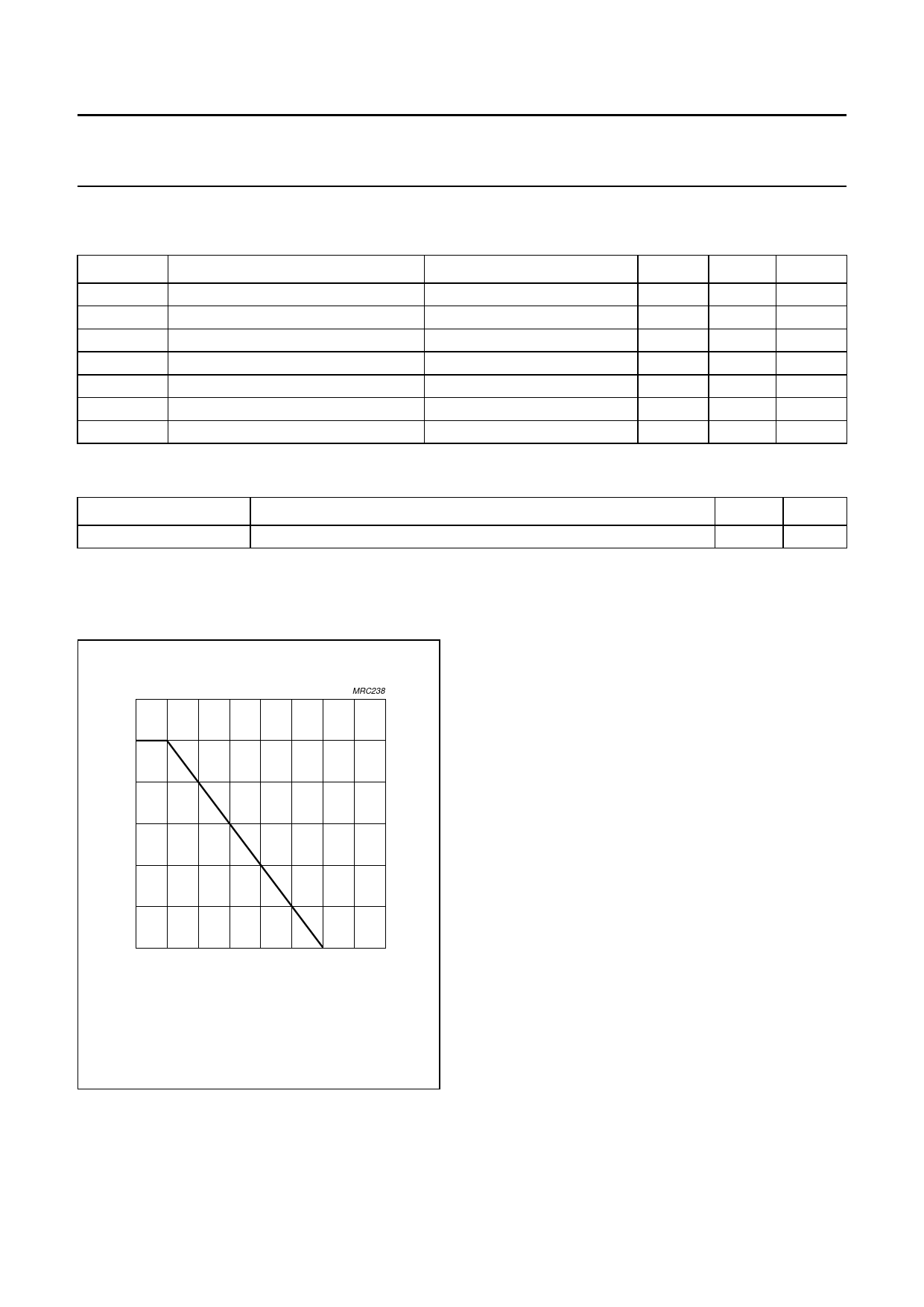
handbook1, .h2alfpage
Ptot
(W)
0.8
MRC238
0.4
0
0
50
100
150
200
Tamb (°C)
Fig.2 Power derating curve.
April 1995
3
Share Link: 