MAX852C/D View Datasheet(PDF) - Maxim Integrated
Part Name
Description
Manufacturer
MAX852C/D Datasheet PDF : 8 Pages
| |||
Low-Noise, Regulated, Negative
Charge-Pump Power Supplies for GaAsFET Bias
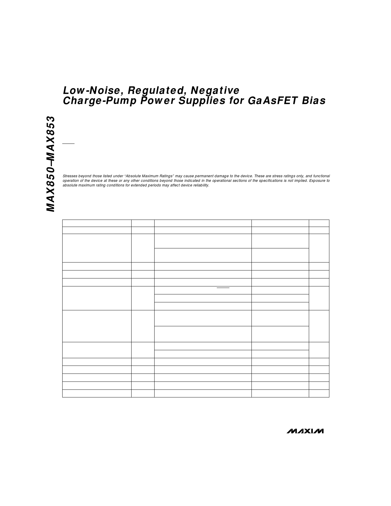
ABSOLUTE MAXIMUM RATINGS
Supply Voltage, VIN to GND ..................................-0.3V to 10.5V
VNEGOUT to GND ...................................................-10.5V to 0.3V
VIN to VNEGOUT .........................................................-0.3V to 21V
VOUT to GND (Note 1) ........................................VNEGOUT to 0.3V
SHDN or OSC (pin 4) Voltage to GND.........-0.3V to (VIN + 0.3V)
Continuous Power Dissipation (TA = +70°C)
SO (derate 5.88mW/°C above +70°C) ........................471mW
Operating Temperature Ranges
MAX85_ISA ......................................................-25°C to +85°C
MAX85_ESA.....................................................-40°C to +85°C
Storage Temperature Range .............................-65°C to +160°C
Lead Temperature (soldering, 10sec) .............................+300°C
Note 1: The output may be shorted to NEGOUT or GND if the package power dissipation is not exceeded. Typical short-circuit
current to GND is 50mA.
Stresses beyond those listed under “Absolute Maximum Ratings” may cause permanent damage to the device. These are stress ratings only, and functional
operation of the device at these or any other conditions beyond those indicated in the operational sections of the specifications is not implied. Exposure to
absolute maximum rating conditions for extended periods may affect device reliability.
ELECTRICAL CHARACTERISTICS
(+5V ≤ VIN ≤ +10V, GND = 0V, VOUT = -4.1V, RL = ∞, TA = TMIN to TMAX, unless otherwise noted. A 100kHz, 50% duty cycle square
wave between GND and VIN is applied to OSC on the MAX852.)
PARAMETER
SYMBOL
CONDITIONS
MIN TYP MAX UNITS
Supply Voltage Range (Note 2)
VIN
5
10
V
Output Voltage
VOUT
MAX850–MAX852, VFB = 0V,
RL = ∞ or 820Ω, Figure 2a
MAX853, VCTRL = 4.1V,
RL = ∞ or 820Ω, Figure 2c
-4.3 -4.1
-3.9
V
-4.2
-4.0
Output Voltage Range
-0.5 to -(VIN - 1)
V
Set Voltage
VFBset MAX850–MAX852, no load, Figure 2b
-1.32 -1.28 -1.24
V
Supply Current
IQ
2.0
3.0
mA
MAX850/MAX853, VIN = 10V, SHDN = 0V
0.002
1
Shutdown Supply Current
ISHUT MAX851, SHDN = 2V
2
5
µA
MAX852, OSC low
1
VOUT Load Regulation
MAX850–MAX852, VFB = 0V,
RL = ∞ or 820Ω, Figure 2a
MAX853, VCTRL = 4.1V,
RL = ∞ or 820Ω, Figure 2c
4
8
mV/mA
3
8
VOUT Ripple
Oscillator Frequency (Note 3)
Input High Voltage
Input Low Voltage
Input Current
Input Capacitance
fOSC
VIH
VIL
IIN
CIN
MAX850–MAX852
MAX853
MAX850/MAX851/MAX853, TA = +25°C
Pin 4
Pin 4
Pin 4
Pin 4
2
mVp-p
1
80
100
120 kHz
2.0
V
0.5
V
±1
µA
10
pF
Note 2: The supply voltage can drop to 4.5V, but the output may no longer sink 5mA at -4.1V.
Note 3: The MAX852 will operate with a 50kHz to 250kHz square wave of 40% to 60% duty cycle. For best performance, use an
80kHz to 120kHz square wave with 50% duty cycle.
2 _____________________________________________________________________________________
Share Link: 