KGF1256B View Datasheet(PDF) - Oki Electric Industry
Part Name
Description
Manufacturer
KGF1256B Datasheet PDF : 14 Pages
| |||
¡ electronic components
KGF1256B/1256
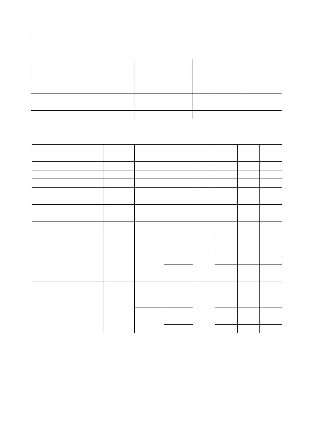
ABSOLUTE MAXIMUM RATINGS
Item
Drain-source voltage
Gate-source voltage
Drain current
Total power dissipation
Channel temperature
Storage temperature
Symbol
VDS
VGS
IDS
Ptot
Tch
Tstg
Condition
Ta = 25°C
Ta = 25°C
Ta = 25°C
Ta = 25°C
—
—
Unit
Min.
V
—
V
–3.0
mA
—
mW
—
°C
—
°C
–45
Max.
7
0.4
360
300
150
125
ELECTRICAL CHARACTERISTICS
Item
Gate-source leakage current
Gate-drain leakage current
Drain-source leakage current
Drain current
Operating current
Gate-source cut-off voltage
Transconductance
Noise figure
Linear gain
Output power
Symbol
IGSS
IGDO
IDS(off)
IDSS
ID
VGS(off)
gm
F
GLIN
PO
Condition
VGS = –3 V
VGD = –11 V
VDS = 3 V, VGS = –2 V
VDS = 3 V, VGS = 0 V
(*1), PIN = 5 dBm,
f = 850 MHz
Unit
mA
mA
mA
mA
mA
VDS = 3 V, IDS = 720 mA
V
VDS = 3 V, IDS = 25 mA
mS
(*1), f = 850 MHz
dB
f = 850 MHz
(*1), PIN =
–20 dBm
f = 1.5 GHz
f = 1.9 GHz
dB
f = 850 MHz
(*2), PIN =
–20 dBm
f = 1.5 GHz
f = 1.9 GHz
f = 850 MHz
(*1), PIN =
5 dBm
f = 1.5 GHz
f = 1.9 GHz
dBm
f = 850 MHz
(*2), PIN =
5 dBm
f = 1.5 GHz
f = 1.9 GHz
*1 Self-bias condition: VDD = 5±0.25 V, VG = 0 V
*2 Self-bias condition: VDD = 3 V, VG = 0 V
Min.
—
—
—
100
—
–1.5
100
—
14.0
—
—
—
—
—
16.0
—
—
—
—
—
(Ta = 25°C)
Typ. Max.
—
72
—
360
—
720
—
—
—
40.0
—
–0.5
—
—
—
2.5
18.0
—
13.0
—
10.5
—
18.0
—
12.5
—
10.0
—
18.0
—
15.5
—
11.5
—
15.0
—
13.0
—
10.5
—
3/14
Share Link: 