2N7002KU View Datasheet(PDF) - GOOD-ARK
Part Name
Description
Manufacturer
2N7002KU Datasheet PDF : 6 Pages
| |||
2N7002KU
60V N-Channel MOSFET
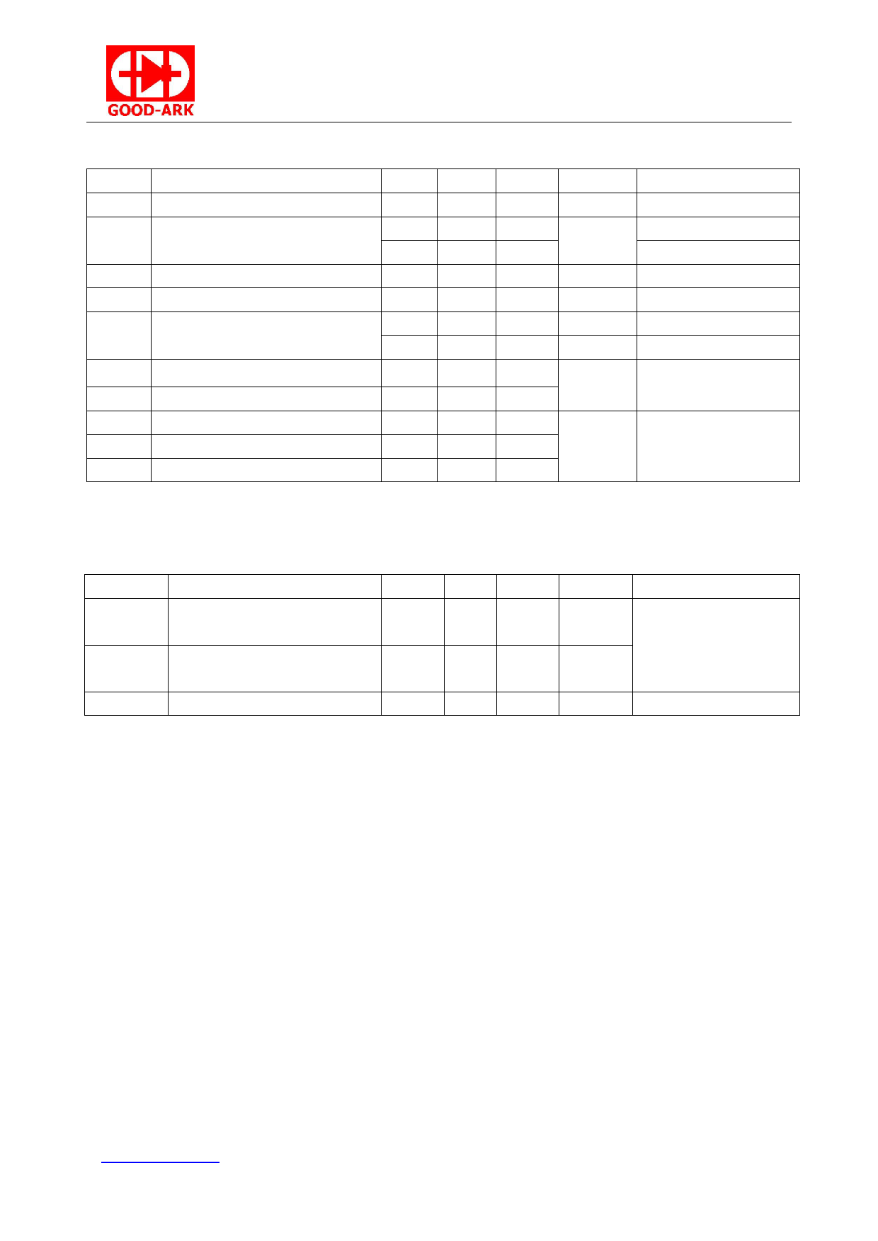
Electrical Characteristics @TA=25℃ unless otherwise specified
Symbol Parameter
Min.
V(BR)DSS Drain-to-Source breakdown voltage 60
—
RDS(on) Static Drain-to-Source on-resistance
—
VGS(th) Gate threshold voltage
1
IDSS
Drain-to-Source leakage current
—
—
IGSS
Gate-to-Source forward leakage
—
td(on)
Turn-on delay time
—
td(off)
Turn-Off delay time
—
Ciss
Input capacitance
—
Coss
Output capacitance
—
Crss
Reverse transfer capacitance
—
Typ.
—
1.6
—
—
—
—
—
—
—
40
16.6
9.5
Max.
—
3
3.5
2.5
1
±100
±10
25
45
—
—
—
Units
V
Ω
V
μA
nA
uA
ns
pF
Conditions
VGS = 0V, ID = 250μA
VGS=10V, ID=0.5A
VGS=5V, ID=0.05A
VDS = VGS, ID = 250μA
VDS = 60V,VGS = 0V
VGS=±5V,VDS=0V
VGS=±20V,VDS=0V
VGS=10V, VDS=30V,
ID=0.2A,RGEN=10Ω
VGS = 0V
VDS = 25V
ƒ = 1MHz
Source-Drain Ratings and Characteristics
Symbol
IS
ISM
VSD
Parameter
Continuous Source Current
(Body Diode)
Pulsed Source Current
(Body Diode)
Diode Forward Voltage
Min. Typ. Max.
—
— 0.3
—
— 1.2
—
— 1.3
Units
A
A
V
Conditions
MOSFET symbol
showing the
integral reverse
p-n junction diode.
IS=0.2A, VGS=0V
www.goodark.com
Page 2 of 6
Rev.1.0
Share Link: 