VSC7185 Ver la hoja de datos (PDF) - Vitesse Semiconductor
Número de pieza
componentes Descripción
Fabricante
VSC7185 Datasheet PDF : 18 Pages
| |||
VITESSE
SEMICONDUCTOR CORPORATION
Preliminary Data Sheet
VSC7185
Quad Transceiver for
Gigabit Ethernet and Fibre Channel
RSYN=0:
RCi0
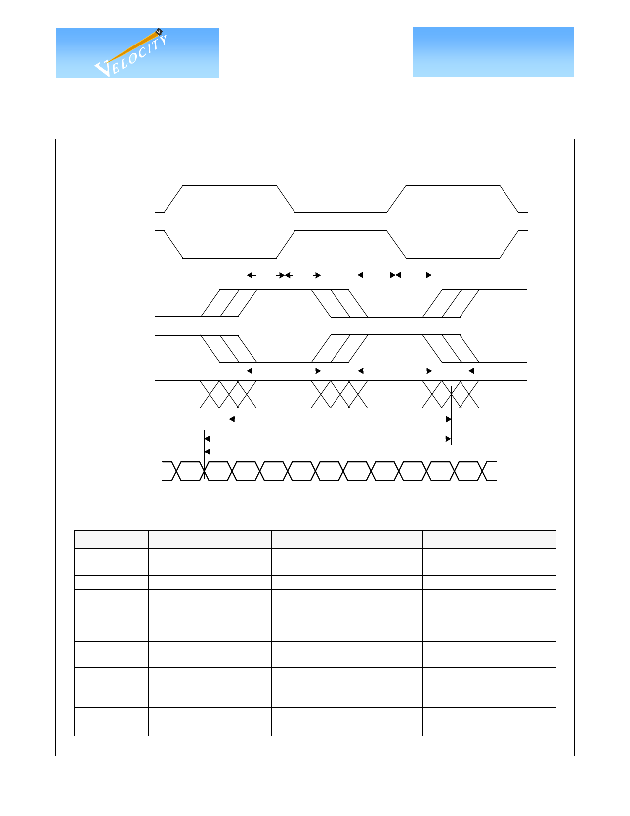
Figure 4: Receive Timing Waveforms
RCi1
RSYN=1:
RCi0
RXS RXH
RXS RXH
RCi1
RXi(0:4)
(SYNi)
SIi+/-
RXCV
RXCT
A[5:9]
B[0:4]
10-BIT CHAR C
RXi0 RXi1 RXi2
10 bit times
RXLAT
RXCV
B[5:9]
RXCT
C[0:4]
Table 3: Receive AC Characteristics
Parameters
f_lock
B_sync
TRXS
TRXH
TRXCT
TRXCV
TRXLAT
Description
Frequency Lock Time from
Power On
Bit Sync Time
RXi(0:4) Setup Time (Data
Valid Before Clock)
RXi(0:4) Hold Time
(Data Valid After Clock)
RXi(0:4) and RCi(0:1)
Transition Range
RX(0:4) and RCi(0:1) Valid
Time
RC0 to RC1 Skew
RC0 or RC1 Duty Cycle
Receiver Latency
Min.
—
—
1.50
Max.
500
2500
—
Units
Conditions
µs
bits
bits RSYN=0
1.50
—
bits RSYN-0
—
1.25
bits RSYN=1
3.75
-0.5
40
18.5 bits + 2 ns
—
+0.5
60
19.5 bits + 5 ns
bits RSYN=1
ns
%
—
G52324-0, Rev. 3.0
8/28/00
© VITESSE SEMICONDUCTOR CORPORATION
741 Calle Plano, Camarillo, CA 93012 • 805/388-3700 • FAX: 805/987-5896
Page 7
Share Link: 