MC3479 Ver la hoja de datos (PDF) - Motorola => Freescale
Número de pieza
componentes Descripción
Fabricante
MC3479 Datasheet PDF : 10 Pages
| |||
MC3479
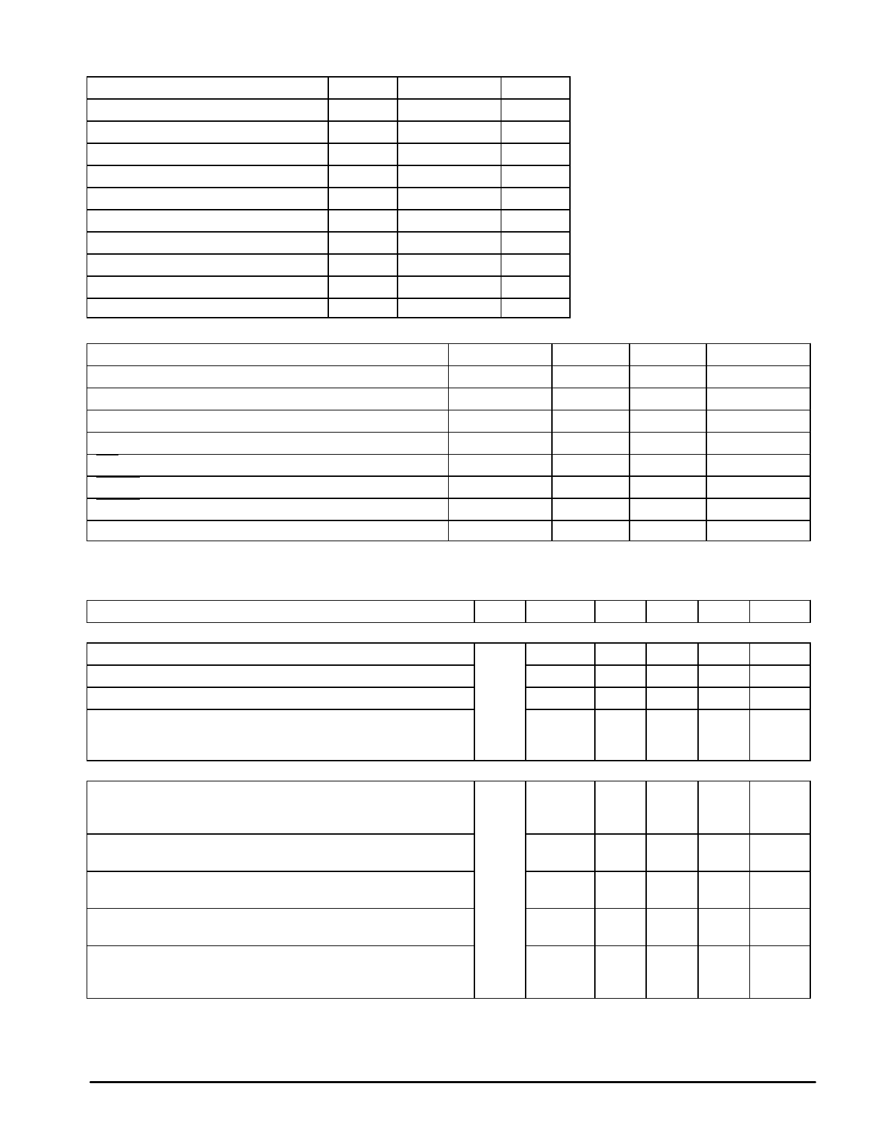
MAXIMUM RATINGS
Rating
Symbol
Value
Unit
Supply Voltage
Clamp Diode Cathode Voltage (Pin 1)
Driver Output Voltage
Drive Output Current/Coil
Input Voltage (Logic Controls)
Bias/Set Current
Phase A Output Voltage
Phase A Sink Current
Junction Temperature
Storage Temperature Range
VM
+ 18
Vdc
VD
VM + 5.0
Vdc
VOD
VM + 6.0
Vdc
IOD
± 500
mA
Vin
– 0.5 to + 7.0
Vdc
IBS
– 10
mA
VOA
+ 18
Vdc
IOA
20
mA
TJ
+ 150
°C
Tstg
– 65 to + 150
°C
RECOMMENDED OPERATING CONDITIONS
Characteristic
Symbol
Min
Max
Unit
Supply Voltage
Clamp Diode Cathode Voltage
Driver Output Current (Per Coil) (Note 1)
Input Voltage (Logic Controls)
Bias/Set Current (Outputs Active)
Phase A Output Voltage
Phase A Sink Current
Operating Ambient Temperature
NOTE: 1. See section on Power Dissipation in Application Information.
VM
VD
IOD
Vin
IBS
VOA
IOA
TA
+ 7.2
+ 16.5
Vdc
VM
VM + 4.5
Vdc
—
350
mA
0
+ 5.5
Vdc
– 300
– 75
µA
—
VM
Vdc
0
8.0
mA
0
+ 70
°C
DC ELECTRICAL CHARACTERISTICS (Specifications apply over the recommended supply voltage and temperature range, [Notes
2, 3] unless otherwise noted.)
Characteristic
Pins Symbol Min
Typ
Max
Unit
INPUT LOGIC LEVELS
Threshold Voltage (Low–to–High)
Threshold Voltage (High–to–Low)
7, 8,
VTLH
—
—
2.0
Vdc
9, 10
VTHL
0.8
—
—
Vdc
Hysteresis
VHYS
0.4
—
—
Vdc
Current: (VI = 0.4 V)
Current: (VI = 5.5 V)
Current: (VI = 2.7 V)
IIL
– 100
—
—
µA
—
—
+ 100
—
—
+ 20
DRIVER OUTPUT LEVELS
Output High Voltage
(IBS = – 300 µA): (IOD = – 350 mA)
(IBS = – 300 µA): (IOD = – 0.1 mA)
2, 3,
VOHD
Vdc
14, 15
VM – 2.0 —
—
VM – 1.2 —
—
Output Low Voltage
(IBS = – 300 µA, IOD = 350 mA)
VOLD
—
—
0.8
Vdc
Differential Mode Output Voltage Difference (Note 4)
(IBS = – 300 µA, IOD = 350 mA)
DVOD
—
—
0.15
Vdc
Common Mode Output Voltage Difference (Note 5)
(IBS = – 300 µA, IOD = – 0.1 mA)
CVOD
—
—
0.15
Vdc
Output Leakage, Hi Z State
p p (0 VOD VM, IBS = – 5.0 µA)
p p (0 VOD VM, IBS = – 300 µA, F/H = 2.0 V, OIC = 0.8 V)
µA
IOZ1
– 100
—
+ 100
IOZ2
– 100
—
+ 100
NOTES: 2. Algebraic convention rather than absolute values is used to designate limit values.
3. Current into a pin is designated as positive. Current out of a pin is designated as negative.
4. DVOD = VOD1,2 – VOD3,4 where: VOD1,2 = (VOHD1 – VOLD2) or (VOHD2 – VOLD1), and
VOD3,4 = (VOHD3 – VOLD4) or (VOHD4 – VOLD3).
5. CVOD = VOHD1 – VOHD2 or VOHD3 – VOHD4.
2
MOTOROLA ANALOG IC DEVICE DATA
Share Link: 