AD7719 Ver la hoja de datos (PDF) - Analog Devices
Número de pieza
componentes Descripción
Fabricante
AD7719 Datasheet PDF : 40 Pages
| |||
AD7719
The serial interface can be reset by exercising the RESET input
on the part. It can also be reset by writing a series of 1s on the
DIN input. If a logic 1 is written to the AD7719 DIN line for at
least 32 serial clock cycles, the serial interface is reset. This ensures
that in 3-wire systems, if the interface gets lost, either via a software
error or by some glitch in the system, it can be reset back to a
known state. This state returns the interface to where the AD7719
is expecting a write operation to its Communications register. This
operation resets the contents of all registers to their power-on
reset values.
Some microprocessor or microcontroller serial interfaces have a
single serial data line. In this case, it is possible to connect the
AD7719’s DATA OUT and DATA IN lines together and connect
them to the single data line of the processor. A 10 kΩ pull-up
resistor should be used on this single data line. In this case, if the
interface gets lost, because the read and write operations share
the same line, the procedure to reset it to a known state is
somewhat different than previously described. It requires a read
operation of 24 serial clocks followed by a write operation where
a logic 1 is written for at least 32 serial clock cycles to ensure
that the serial interface is back in a known state.
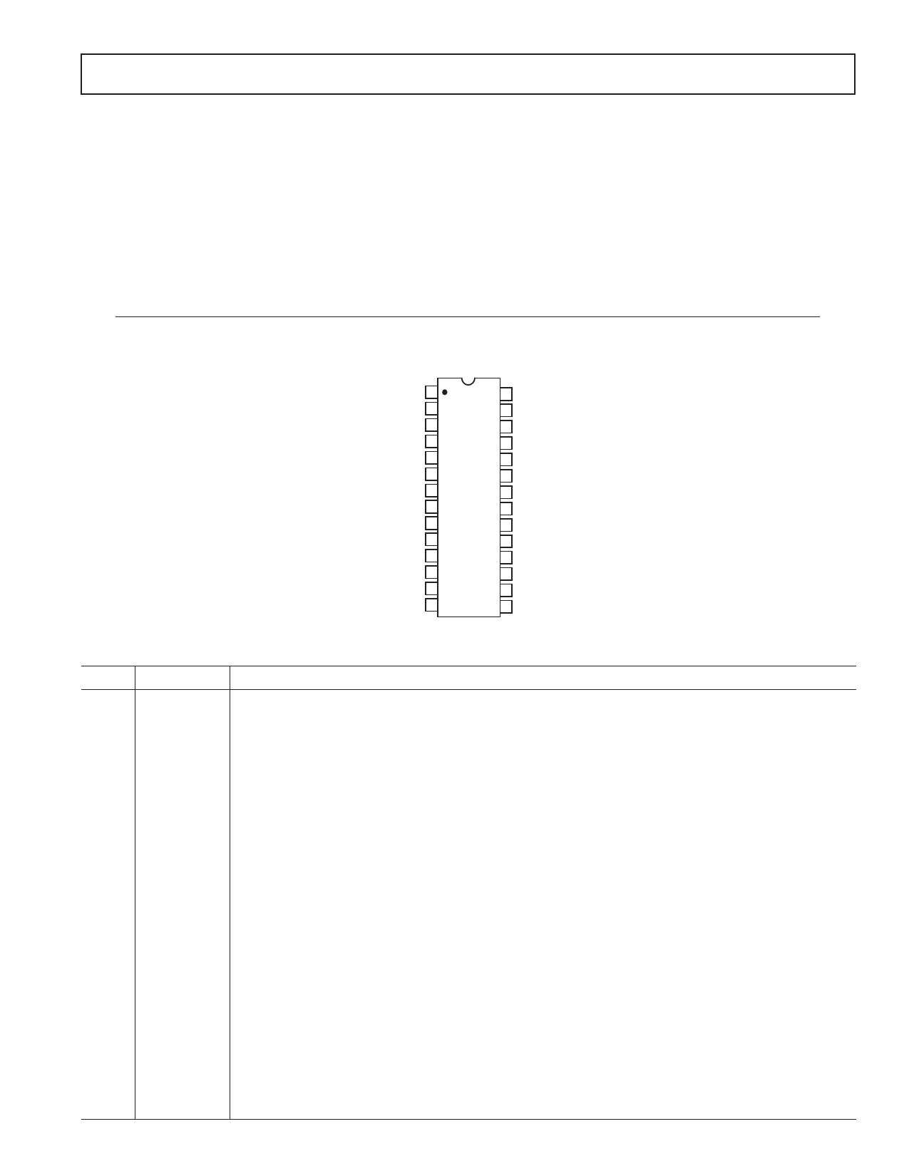
PIN CONFIGURATION
IOUT1 1
28 XTAL1
IOUT2 2
27 XTAL2
AVDD 3
AGND 4
26 DVDD
25 DGND
REFIN1(–)
REFIN1(+)
AIN1
5 AD7719 24 DIN
6 TOP VIEW 23 DOUT
7 (Not to Scale) 22 RDY
AIN2 8
21 CS
AIN3 9
20 SCLK
AIN4 10
19 RESET
AIN5 11
18 P1/SW1
AIN6 12
17 PWRGND
REFIN2 13
16 P2/SW2
P4 14
15 P3
Pin No. Mnemonic
1
IOUT1
2
IOUT2
3
AVDD
4
AGND
5
REFIN1(–)
6
REFIN1(+)
7
AIN1
8
AIN2
9
AIN3
10
AIN4
11
AIN5
12
AIN6
13
REFIN2
14
P4
15
P3
REV. A
PIN FUNCTION DESCRIPTIONS
Function
Output for Internal 200 µA Excitation Current Source. Current source IEXC1 and/or IEXC2 can be
switched to this output.
Output for Internal 200 µA Excitation Current Source. Current source IEXC1 and/or IEXC2 can be
switched to this output.
Analog Supply Voltage.
Analog Ground.
Negative Reference Input for Main ADC Channel. This reference input can lie anywhere between AGND
and AVDD – 1 V.
Positive Reference Input for Main ADC Channel. REFIN1(+) can lie anywhere between AVDD and
AGND + 1 V. The nominal reference voltage (REFIN1(+) – REFIN1(–)) is 2.5 V, but the part is functional
with a reference range from 1 V to AVDD.
Analog Input. AIN1 is dedicated to the main channel.
Analog Input. AIN2 is dedicated to the main channel.
Analog Input. AIN3 can be multiplexed to either the main or auxiliary channel.
Analog Input. AIN4 can be multiplexed to either the main or auxiliary channel.
Analog Input. AIN5 is dedicated to the auxiliary channel and is referenced to AIN6 or AGND.
Analog Input. AIN6 is dedicated to the auxiliary channel. It forms a differential input pair with AIN5 in
fully differential input mode or is referenced to AGND in pseudodifferential mode.
Single-Ended Reference Input for Auxiliary Channel. The nominal input reference is 2.5 V. The auxiliary
channel will function with an input reference range from 1 V to AVDD.
General-Purpose I/O Bit. The input and output voltage levels are referenced to AVDD and AGND.
General-Purpose I/O Bit. The input and output voltage levels are referenced to AVDD and AGND.
–9–
Share Link: 